M.sc I-sem-8086 notes
•Transferir como DOC, PDF•
4 gostaram•801 visualizações

class notes for M.Sc I sem electronics students on Microcomputer,microprocessor,evolution,types etc...[source:David.V.Hall]

Recomendados
Recomendados
Mais conteúdo relacionado
Mais procurados
Mais procurados (19)
Destaque
Destaque (20)
Semelhante a M.sc I-sem-8086 notes
Semelhante a M.sc I-sem-8086 notes (20)
Mais de Dr.YNM
Mais de Dr.YNM (20)
Último
Último (20)
M.sc I-sem-8086 notes
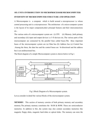
- 1. 103: UNIT-I INTRODUCTION TO MICROPROCESSOR/MICROCOMPUTER OVERVIEW OF MICROCOMPUTER STRUCTURE AND OPERATION A Microcomputer is a computer which is build around a microprocessor i.e whose central processing unit is a microprocessor. The architecture of a micro-computer system is the layout of its major components,their principal features and their interconnections etc.. The various units of a microcomputer system are (i) CPU (ii) Memory ,both primary and secondary (iii) input and output devices i.e I /O devices etc..The various parts of the microcomputer are connected by the parallel lines called buses.The three important buses of the microcomputer system are (a) Data bus (b) Address bus (c) Control bus .Among the three, the data bus and the control buses are bi-directional and the address bus is an unidirectional bus. The block diagram of a simple Microcomputer system is shown below in Fig.1. Fig.1.Block Diagram of a Microcomputer system. Let us consider in detail the various blocks of the microcomputer system. MEMORY: This section of memory consists of both primary memory and secondary memory.The primary memory constitutes the RAM & ROM. These are semiconductor memories. In addition to this ,the system may also contain secondary memories like magnetic floppy disks, magnetic hard disks or optical disks. The memory can store the
- 2. binary codes for the sequences of instructions and also the binary coded data with which the computer is going to work. INPUT/OUTPUT: The I/O section allows to input the data in to the computer and sends the data to the outside world after necessary processing. The peripherals such as keyboards, video display terminals, printers and modems are considered as I/O devices. These devices allow the user and the computer to communicate with each other. The actual electronic circuitary used to interface the computer buses to external devices are often called ports. The input port allows data from a keyboard, to be read in to the computer under the control of CPU. An O/P Port is used to send data from the computer to some peripheral like display terminal, a printer, or a D/A converter etc..In practice ,the ports of a computer is nothing but a set of D-flip-flops. CENTRAL PROCESSING UNIT : All the operations of the computer are performed under the control of the central processing unit(CPU). The CPU fetches binary coded instructions from memory, decodes the instructions into a series of simple actions and executes these actions in a sequence of steps. The CPU also contains an address counter or instruction pointer register which holds the address of the next instruction, to be executed . The CPU contains certain general purpose registers (GPRs) which are used for temporary storage of binary data and also contains the control circuitry which generates the control bus signals. The system bus of the microcomputer constitutes three buses .They are Address bus,Data bus and control bus. ADDRESS BUS : The address bus consists of 16,20,24,32 parallel signal lines. On these lines the CPU sends out the address of the memory location. If the CPU has N address lines then it can directly address 2N memory locations.For example with 16 bit address bus the CPU can address a memory space of 216 = 64 kB(65,536) DATA BUS- The data bus consists of 8, 16, or 32 parallel signal lines. The data bus is a bi-directional bus.The double ended arrows on the data bus indicates that the CPU can read data in from memory or from a port on these lines, or it can send data out to memory
- 3. or to a port on these lines. Any device connected to this data bus must have tri-state outputs so that its outputs can be disabled when it is not being used. CONTROL BUS- The control bus which is also bi-directional ,consists of 4 to 10 parallel signal lines. The CPU sends out signals on the control bus to enable the outputs of addressed memory devices or port devices. Typical control bus signals are memory read, memory write, I/O read, and I/O write. To read a byte of data from a memory location, the CPU sends out the memory address of the desired byte on the address bus and then sends out the memory read signal on the control bus. The memory read signal enables the addressed memory device to output a data word on to the data bus. The data word from the memory travels along the data bus to the CPU. OPERATION: The operation of the microcomputer system can be explained broadly in the following steps. (a).The microcomputer fetches each program instruction in sequence ,decodes it and then executes the instruction. (b)The CPU of the microcomputer fetches instructions or reads data from memory by sending out an address on the address bus and memory read signal on the control bus. The memory outputs the addressed instruction or data word to the CPU on the data bus. (c).The CPU of the microcomputer fetches instructions or read data from memory by sending out an address on the address bus and a memory read signal on the control bus. The memory outputs the addressed instruction or data to the CPU on the data bus. (d).The CPU writes data word to memory by sending out an address on the address bus ,and sending the data on the data bus and sending a memory write signal to memory on the control bus. (e)To read the data from a port the CPU sends out the port address on the address bus and sends an I/O read signal to the port device on the control bus.The data from the port comes into the CPU on the data bus.
- 4. (f). To write data to a port ,the CPU sends out the port address on the address bus ,also sends the data to be written to the port on the data bus and sends an I/O write signal to the port device on the control bus. IDEAL MICROPROCESSOR: An ideal microprocessor is only a hypothetical device which contains the complete set of input, out lines ,memory and all the other necessary ports on the same chip. The internal ROM stores the sequence of instructions known as program in the binary code. The input signals are applied at the input pins and are processed according to the instructions of the program and the output in the binary should be available at the output pins. The m input and n output ideal microprocessor with internal ROM is shown in the figure below. Fig 2.Ideal Microprocessor The concept of ideal microprocessor is not practically possible due to many constraints. For example,in a 8085 microprocessor there are 8 data lines and 16 address lines .So ,to fabricate an ideal 8085 microprocessor one has to use 8-pins for data and 16-pins for address lines.If this is followed ,the total number of pins increases drastically as a result of which the size and complexity and also the cost of the IC increases. Also it is not possible to provide large amount of on chip memory and large number of I/O ports. So,in all practical or real microprocessors ,using the multiplexing concept the number of I/O pins is reduced and also small amount of memory is introduced so that both the size and
- 5. the cost of the processor reduces. A programmable peripheral interface is used for I/O ports. This will reduce the size and cost of the microprocessor. Due to the above said reasons, the concept of ideal microprocessor is only a hypothetical and not practically possible. MICROPROCESSOR EVOLUTION AND TYPES: EVOLUTION : The first Microprocessor (4004) was designed by Intel Corporation which was founded by Moore and Noyce in 1968. In the early years, Intel focused on developing semiconductor memories (DRAMs and EPROMs) for digital computers. In 1969, a Japanese Calculator manufacturer, Busicom approached Intel with a design for a small calculator which need 12 custom chips. Ted Hoff, an Intel Engineer thought that a general purpose logic device could replace the multiple components. This idea led to the development of the first so called microprocessor. So, Microprocessors started with a modest beginning of drivers for calculators. Fedrico Faggin and Stanely Mazor implemented the ideas of Ted Hoff’s and designed the Intel 4000 family of processors comprising 4001 (2K-ROM), the 4002 (320 bit RAM), the 4003 (10 bit I/O shift-register) and the 4004, a 4 bit CPU. Intel introduced the 4004 microprocessor to the world wide market on November 15, 1971. It was a 4-bit PMOS chip with 2300 transistors. Around the same time Texas Instruments developed a 4-bit microprocessor TMS 1000 and became the owner of microprocessor patent. Later Intel introduced world’s first 8 bit general purpose microprocessor 8008 in 1972. This processor was used in the popular computer ‘Mark-8’ in those days. In 1974, Intel introduced the improved version of 8008, the 8080 microprocessor. This 8080 is the much more highly integrated chip than its predecessors which is built around N-channel MOS technology. It could execute up to 290,000 operations per second and could address up to 64K.bytes of memory. During the same time Motorola introduced the 8-bit microprocessor Motorola 6800, and Rockwell PPS-8 and Signetics 2650 with powerful architecture and instruction set. With developments in integration technology Intel was able to integrate the additional chips like 8224 clock generator and the 8228 system controller along with
- 6. 8080 microprocessor with in a single chip and released the 8 bit microprocessor 8085 in the year 1976. The 8085 microprocessor consisted of 6500 MOS transistors and could work at clock frequencies of 3-5 MHz. It works on a single +5 volts supply. The other improved 8 bit microprocessors from the Motorola company is MC 6809,from ZILOG company is Zilog Z-80 and from RCA is COSMAC. In 1978, Intel introduced the 16 bit microprocessor 8086 and 8088 in 1979. IBM selected the Intel 8088 for their personal computer (IBM-PC).8086 microprocessor made up of 29,000 MOS transistors and could work at a clock speed of 5-10 MHz. It has a 16-bit ALU with 16-bit data bus and 20-bit address bus. It can address up to 1MB of address space. The pipelining concept was used for the first time to improve the speed of the processor. It had a pre-fetch queue of 6 instructions where in the instructions to be executed were fetched during the execution of an instruction. It means 8086 architecture supports parallel processing. The 8088 microprocessor is similar to 8086 processor in architecture ,but the basic difference is it has only 8-bit data bus even though the ALU is of 16-bit.It has a pre-fetch queue of 4-instructions only. In 1982 Intel released another 16-bit processor called 80186 designed by a team under the leadership of Dave Stamm. This is having higher reliability and faster operational speed but at a lower cost. It had a pre-fetch queue of 6-instructions and it is suitable for high volume applications such as computer workstations, word-processor and personal computers. It is made up of 134,000 MOS transistors and could work at clock rates of 4 and 6 MHz. This is also comes under first generation of Microprocessors. Intel released another 16 bit microprocessor 80286 having 1, 34,000 transistors in 1982. It was used as CPU in PC-ATs in 1982. It is the second generation microprocessor, more advanced to 80186 processor. It could run at clock speeds of 6 to 12.5 MHz .It has a 16-bit data bus and 24-bit address bus, so that it can address up to 16MB of address space and 1GB of virtual memory. It had a pre-fetch queue of 6 instructions .Intel introduced the concept of protected mode and virtual mode to ensure
- 7. proper operation. It also had on-chip memory management unit (MMU) .This was popularly called as Intel 286 in those days. In 1985, Intel released the first 32 bit processor 80386, with 275,000 transistors. It has 32-bit data bus and 32-bit address bus so that it can address up to a total of 4GB memory also a virtual memory space of 64TB.It could process five million instructions per second and could work with all popular operating systems including Windows. It has a pre-fetch queue of length 16-bytes with extensive memory management capabilities. It is incorporated with a concept called paging in addition to segmentation technique. It uses a math co-processor called 80387. Intel introduced 80486 microprocessor in the year 1989, with a built-in maths co-processor and with 1.2 million transistors. It could run at the clock speed of 50 MHz This is also a 32 bit processor but it is twice as fast as 80386.The additional features in 486 processor are the built-in Cache of 8kB and built-in math co-processors. The address bus here is bidirectional because of presence of cache memory. On 19th October, 1992, Intel released the Pentium-I Processor with 3.1 million transistors. So, the Pentium began as fifth generation of the Intel x86 architecture. This Pentium was a backward compatible while offering new features. The revolutionary technology followed is that the CPU is able to execute two instruction at the same time. This is known as super scalar technology. The Pentium uses a 32-bit expansion bus, however the data bus is 64 bits. The 7.5 million transistors based chip, Intel Pentium II processor was released in 1997. It works at a clock speed of 300M.Hz. Pentium II uses the Dynamic Execution Technology which consists of three different facilities namely, Multiple branch prediction, Data flow analysis, and Speculative execution unit. Another important feature is a thermal sensor located on the mother board can monitor the die temperature of the processor. For thermal management applications.
- 8. Intel Celeron Processors were introduced in the year 1999. Pentium-III processor with 9.5 million transistors was introduced in 1999. It also uses dynamic execution micro- architecture, a unique combination of multiple branch prediction, dataflow analysis and speculative execution. The Pentium III has improved MMX and processor serial number feature. The improved MMX enables advanced imaging, 3D streaming audio and video, and speech recognition for enhanced Internet facility. Pentium-IV with 42 million transistors and 1.5 GHz clock speed was released by Intel in November 2000. The Pentium 4 processor has a system bus with 3.2 G-bytes per second of bandwidth. This high bandwidth is a key reason for applications that stream data from memory. This bandwidth is achieved with 64 –bit wide bus capable of transferring data at a rate of 400 MHz. The Pentium 4 processor enables real-time MPEG2 video encoding and near real-time MPEG4 encoding, allowing efficient video editing and video conferencing. Intel with partner Hewlett-Packard developed the next generation 64-bit processor architecture called IA-64 .This first implementation was named Itanium. Itanium processor which is the first in a family of 64 bit products was introduced in the year 2001.The Itanium processor was specially designed to provide a very high level of parallel processing ,to enable high performance without requiring very high clock frequencies .Key strengths of the Itanium architecture include ,up to 6 instructions/cycle. The Itanium processor can handle up to 6 simultaneous 64 –bit instructions per clock cycle. The Itanium II is an IA-64 microprocessor developed jointly by Hewlett-Packard (HP) and Intel and released on July 8,2002..It is theoretically capable of performing nearly 8 times more work per clock cycle than other CISC and RISC architectures due to its parallel computing micro-architecture. The recent Itanium processor features a split L2 cache, adding a dedicated 1MB L2 cache for instructions and thereby effectively growing the original 256KBL2 cache, which becomes a dedicated data cache. The first Itanium 2
- 9. processor (code named McKinley) was more powerful than the original Itanium processor, with approximately two times performance. Pentium 4EE was released by Intel in the year 2003 and Pentium 4E was released in the year 2004. The Pentium Dual-Core brand was used for mainstream X86-architecture microprocessors from Intel from 2006 to 2009 The 64 bit Intel Core2 was released on July 27, 2006. In terms of features, price and performance at a given clock frequency, Pentium Dual-Core processors were positioned above Celeron but below Core and Core 2 microprocessors in Intel's product range. The Pentium Dual-Core was also a very popular choice for over clocking, as it can deliver optimal performance (when over clocked) at a low price. The Pentium Dual Core, which consists of 167 million transistors was released on January 21, 2007. Intel Core Duo consists of two cores on one die, a 2 MB L2 cache shared by both cores, and an arbiter bus that controls both L2 cache and FSB access. Core 2 Quad processors are multi-chip modules consisting of two dies similar to those used in Core 2 Duo, forming a quad-core processor. While this allows twice the performance to a dual- core processors at the same clock frequency in ideal conditions, this is highly workload specific and requires applications to take advantage of the extra cores. In September.2009, new Core i7 models based on the Lynnfield desktop quad- core processor and the Clarksfield quad-core mobile were added, and models based on the Arrandale dual-core mobile processor have been announced. The first six-core processor in the Core lineup is the Gulftown, which was launched on March 16, 2010. Both the regular Core i7 and the Extreme Edition are advertised as five stars in the Intel Processor Rating. TYPES : Today there are various types of microprocessors available in the market.They are classified in to different groups based on the bit length that the ALU can process in one clock cycle. Foe example, a microprocessor with a 4-bit ALU is referred to as a 4- bit microprocessor, regardless of the number of address lines or the number of data lines that it has. Similarly 8-bit, 16 bit, 32bit and 64 etc. Based on the performance also
- 10. microprocessors are classified. They are , dedicated and embedded controllers, bit-slice processors and general purpose CPUs etc.. TECHNOLOGIES USED: The early microprocessors like 4004 were fabricated using PMOS technology. Later INTEL used N-MOS technology and H-MOS technology to fabricate 8085 and 8086 microprocessors. Soon this was changed to CMOS technology which was a very popular fabrication technology used for all the advanced microprocessors.Later on this technology is replaced by BiCMOS technology which has the properties of both bipolar and CMOS technologies.Even today most of the processors are fabricated using this technology. But recently there is advanced BiCMOS technology (ABT) under discussion and may emerge as a promising technology in the processor industry. OVERVIEW OF 8086 MICROPROCESSOR FAMILY: In the 8086 microprocessor family we consider all the advanced microprocessors like INTEL 8088, 80186, 80286, 80386 ,80486 processors. The Intel 8086 is a 16-bit processor that works as a CPU in a microcomputer. The term 16-bit means that it’s ALU, its internal registers, and most of its instructions are designed to work with 16-bit binary words. The 8086 has 16-bit data bus, so it can read data from or write data to memory and ports either16 bits or 8 bits at a time. The 8086 has a 20-bit address bus, so it can address any one of 220 = 1,048,576, memory locations. Sixteen bit words will be stored in two consecutive memory locations. If the first byte of the word is at an even address, the 8086 can read the entire word in one operation. If the first byte of the word is at an odd address, the 8086 will read the first byte with one bus operation and the second byte with another bus operation . The Intel 8088 has the same ALU, the same registers, and the same instruction set as that of 8086 processor. The 8088 has also a 20 bit address bus, so that it can address any one of 1,048,576 bytes in memory. But 8088 processor has only 8 bit data bus so it can only read data from or write data to memory and ports, of 8 bits at a time. The Intel 8088 was used as the CPU in the original IBM personal computers(PC/XT). The Intel 80186 is an improved version of the 8086 and 80188 is the improved version of 8088. In addition to the 16 bit CPU 80186 and 80188 have programmable
- 11. peripheral devices integrated in the same package. The instruction set of 80186/80188 is a super set of the instruction set of 8086.I.e a program written for 8086/8088 will certainly excute on 80186 or 80188 microprocessors but the converse is not true. The Intel 80286 is a 16 bit ,advanced version of the 8086 which is specifically designed for use as a CPU in a multi-user or multitasking microcomputer. When operating in its real address mode 80286 works mostly as a fast 8086. Most programs written for 8086 can run on an 80286 operating in its real address mode. The 80286 processor was used in IBM PC/AT computers as the CPU. The Intel 80386 is the first 32 bit microprocessor which is upward compatible from the 8086 ,80186 and 80286.It can directly address up to 4 gigabytes of memory. This 80386 contains more sophisticated features than 80286 processor which makes it to work in multi-user and multitasking applications. The architecture of 80386 is known as IA-32 architecture. This architecture extended all the address and general purpose registers to 32 bits, which gave the processor the capability to handle 32 bit address, with 32 bit data. The Intel 80486 is also a 32-bit microprocessor .This is the next member of the IA-32 architecture. This processor has the floating point processor integrated into CPU itself. The 80486 processor consists of an 8kB code and data cache memory. It has a five stage instruction pipeline scheme which allows this to execute instructions much faster than 80386.The 80486 has 6 additional instructions when compared t0 80386 processor. ARCHITECTURE OF INTEL8086/8088: