Mais conteúdo relacionado Semelhante a Lmh6321 (20) 1. LMH6321
www.ti.com SNOSAL8B – APRIL 2006 – REVISED APRIL 2007
LMH6321 300 mA High Speed Buffer with Adjustable Current Limit
Check for Samples: LMH6321
1FEATURES • High capacitive load drive
•
2 High slew rate 1800 V/μs • Thermal shutdown error flag
• Wide bandwidth 110 MHz
APPLICATIONS
• Continuous output current ±300 mA
• Output current limit tolerance ±5 mA ±5% • Line driver
• Wide supply voltage range 5V to ±15V • Pin driver
• Wide temperature range −40°C to +125°C • Sonar driver
• Adjustable current limit • Motor control
DESCRIPTION
The LMH6321 is a high speed unity gain buffer that slews at 1800 V/µs and has a small signal bandwidth of 110
MHz while driving a 50Ω load. It can drive ±300 mA continuously and will not oscillate while driving large
capacitive loads.
The LMH6321 features an adjustable current limit. The current limit is continuously adjustable from 10 mA to 300
ma with a ±5 mA ±5% accuracy. The current limit is set by adjusting an external reference current with a resistor.
The current can be easily and instantly adjusted, as needed by connecting the resistor to a DAC to form the
reference current. The sourcing and sinking currents share the same current limit.
The LMH6321 is available in a space saving 8-pin PSOP or a 7-pin TO-263 power package. The PSOP package
features an exposed pad on the bottom of the package to increase its heat sinking capability. The LMH6321 can
be used within the feedback loop of an operational amplifier to boost the current output or as a stand alone
buffer.
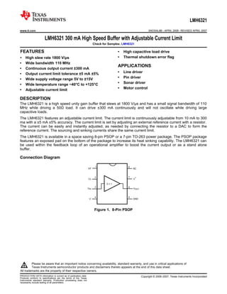
Connection Diagram
1 8
EF NC
2 7 +
CL V
G=1
3 6
VIN VOUT
- 4 5
V GND
Figure 1. 8-Pin PSOP
1
Please be aware that an important notice concerning availability, standard warranty, and use in critical applications of
Texas Instruments semiconductor products and disclaimers thereto appears at the end of this data sheet.
2 All trademarks are the property of their respective owners.
PRODUCTION DATA information is current as of publication date. Copyright © 2006–2007, Texas Instruments Incorporated
Products conform to specifications per the terms of the Texas
Instruments standard warranty. Production processing does not
necessarily include testing of all parameters.
2. LMH6321
SNOSAL8B – APRIL 2006 – REVISED APRIL 2007 www.ti.com
G=1
1 2 3 4 5 6 7
VOUT
+
GND
EF
CL
VIN
-
V
V
A. V− pin is connected to tab on back of each package.
Figure 2. 7-Pin TO-263(A)
These devices have limited built-in ESD protection. The leads should be shorted together or the device placed in conductive foam
during storage or handling to prevent electrostatic damage to the MOS gates.
Absolute Maximum Ratings (1)
(2)
ESD Tolerance
Human Body Model 2.5 kV
Machine Model 250V
Supply Voltage 36V (±18V)
(3)
Input to Output Voltage ±5V
Input Voltage ±VSUPPLY
(4)
Output Short-Circuit to GND Continuous
Storage Temperature Range −65°C to +150°C
Junction Temperature (TJMAX) +150°C
Lead Temperature
(Soldering, 10 seconds) 260°C
(5)
Power Dissipation
CL Pin to GND Voltage ±1.2V
(1) Absolute Maximum Ratings indicate limits beyond which damage to the device may occur. Operating Ratings indicate conditions for
which the device is intended to be functional, but specific performance is not guaranteed. For guaranteed specifications and the test
conditions, see the Electrical Characteristics Table.
(2) Human Body Model is 1.5 kΩ in series with 100 pF. Machine Model is 0Ω in series with 200 pF.
(3) If the input-output voltage differential exceeds ±5V, internal clamping diodes will turn on. The current through these diodes should be
limited to 5 mA max. Thus for an input voltage of ±15V and the output shorted to ground, a minimum of 2 kΩ should be placed in series
with the input.
(4) The maximum continuous current must be limited to 300 mA. See the Application Hints section for more details.
(5) The maximum power dissipation is a function of TJ(MAX), θJA, and TA. The maximum allowable power dissipation at any ambient
temperature is PD = TJ(MAX)–TA)/θJA. See Thermal Management section of the Application Hints.
Operating Ratings
Operating Temperature Range −40°C to +125°C
Operating Supply Range 5V to ±16V
Thermal Resistance (θJA),
(1)
PSOP Package 180°C/W
Thermal Resistance (θJC)
TO-263 Package 4°C/W
Thermal Resistance (θJA)
TO-263 Package 80°C/W
(1) Soldered to PC board with copper foot print equal to DAP size. Natural convection (no air flow). Board material is FR-4.
2 Submit Documentation Feedback Copyright © 2006–2007, Texas Instruments Incorporated
Product Folder Links: LMH6321
3. LMH6321
www.ti.com SNOSAL8B – APRIL 2006 – REVISED APRIL 2007
±15V Electrical Characteristics
The following specifications apply for Supply Voltage = ±15V, VCM = 0, RL ≥ 100 kΩ and RS = 50Ω, CL open, unless otherwise
noted. Boldface limits apply for TA = TJ = TMIN to TMAX; all other limits TA = TJ = 25°C.
Symbol Parameter Conditions Min Typ Max Units
AV Voltage Gain RL = 1 kΩ, VIN = ±10V 0.99 0.995
V/V
0.98
RL = 50Ω, VIN = ±10V 0.86 0.92
V/V
0.84
VOS Input Offset Voltage RL = 1 kΩ, RS = 0V ±4 ±35
mV
±52
IB Input Bias Current VIN = 0V, RL = 1 kΩ, RS = 0V ±2 ±15
μA
±17
R.IN Input Resistance R.L = 50Ω 250 kΩ
CIN Input Capacitance 3.5 pF
RO Output Resistance IO = ±10 mA 5 Ω
IS Power Supply Current RL = ∞, VIN = 0 11 14.5
16.5
mA
750 µA into 14.9 18.5
CL Pin 20.5
VO1 Positive Output Swing IO = 300 mA, RS = 0V, VIN = ±VS 11.2 11.9
10.8
V
Negative Output Swing IO = 300 mA, RS = 0V, VIN = ±VS −11.3 −10.3
−9.8
VO2 Positive Output Swing RL = 1 kΩ, RS = 0V, VIN = ±VS 13.1 13.4
12.9
V
Negative Output Swing RL = 1 kΩ, RS = 0V, VIN = ±VS −13.4 −12.9
−12.6
VO3 Positive Output Swing RL = 50Ω, RS = 0V, VIN = ±VS 11.6 12.2
11.2
V
Negative Output Swing RL = 50Ω, RS = 0V, VIN = ±VS −11.9 −10.9
−10.6
VEF Error Flag Output Voltage RL = ∞, VIN = 0, Normal 5.00
EF pulled up with 5 kΩ
During 0.25 V
to +5V
Thermal
Shutdown
TSH Thermal Shutdown Temperature Measure Quantity is Die (Junction) 168
Temperature °C
Hysteresis 10
ISH Supply Current at Thermal EF pulled up with 5 kΩ to +5V 3 mA
Shutdown
PSSR Power Supply Rejection Ratio RL = 1 kΩ, VIN = 0V, Positive 58 66
VS = ±5V to ±15V 54
dB
Negative 58 64
54
SR Slew Rate VIN = ±11V, RL = 1 kΩ 2900
V/μs
VIN = ±11V, RL = 50Ω 1800
BW −3 dB Bandwidth VIN = ±20 mVPP, RL = 50Ω 110 MHz
LSBW Large Signal Bandwidth VIN = 2 VPP, RL = 50Ω 48 MHz
nd
HD2 2 Harmonic Distortion VO = 2 VPP, f = 100 kHz RL = 50Ω −59
RL = 100Ω −70
dBc
VO = 2 VPP, f = 1 MHz RL = 50Ω −57
RL = 100Ω −68
Copyright © 2006–2007, Texas Instruments Incorporated Submit Documentation Feedback 3
Product Folder Links: LMH6321
4. LMH6321
SNOSAL8B – APRIL 2006 – REVISED APRIL 2007 www.ti.com
±15V Electrical Characteristics (continued)
The following specifications apply for Supply Voltage = ±15V, VCM = 0, RL ≥ 100 kΩ and RS = 50Ω, CL open, unless otherwise
noted. Boldface limits apply for TA = TJ = TMIN to TMAX; all other limits TA = TJ = 25°C.
Symbol Parameter Conditions Min Typ Max Units
HD3 3rd Harmonic Distortion VO = 2 VPP, f = 100 kHz RL = 50Ω −59
RL = 100Ω −70
dBc
VO = 2 VPP, f = 1 MHz RL = 50Ω −62
RL = 100Ω −73
en Input Voltage Noise f ≥ 10 kHz 2.8 nV/
in Input Current Noise f ≥ 10 kHz 2.4 pA/
ISC1 Output Short Circuit Current VO = 0V, Sourcing 4.5 10 15.5
Source (1) Program Current VIN = +3V 4.5 15.5
into CL = 25 µA mA
Sinking 4.5 10 15.5
VIN = −3V 4.5 15.5
VO = 0V Sourcing 280 295 308
Program Current VIN = +3V 273 325
into CL = 750 µA mA
Sinking 280 295 310
VIN = −3V 275 325
ISC2 Output Short Circuit Current RS = 0V, VIN = +3V (1) (2) 320 570 750
Source 300 920
mA
Output Short Circuit Current Sink RS = 0V, VIN = −3V (1) (2) 300 515 750
305 910
V/I Section
CLVOS Current Limit Input Offset Voltage RL = 1 kΩ, GND = 0V ±0.5 ±4.0
mV
±8.0
CLIB Current Limit Input Bias Current RL = 1 kΩ −0.5 −0.2
μA
−0.8
CL Current Limit Common Mode RL = 1 kΩ, GND = −13 to +14V 60 69
dB
CMRR Rejection Ratio 56
(1) VIN = + or −4V at TJ = −40°C.
(2) For the condition where the CL pin is left open the output current should not be continuous, but instead, should be limited to low duty
cycle pulse mode such that the RMS output current is less than or equal to 300 mA.
4 Submit Documentation Feedback Copyright © 2006–2007, Texas Instruments Incorporated
Product Folder Links: LMH6321
5. LMH6321
www.ti.com SNOSAL8B – APRIL 2006 – REVISED APRIL 2007
±5V Electrical Characteristics
The following specifications apply for Supply Voltage = ±5V, VCM = 0, RL ≥ 100 kΩ and RS = 50Ω, CL Open, unless otherwise
noted. Boldface limits apply for TA = TJ = TMIN to TMAX; all other limits TA = TJ = 25°C.
Symbol Parameter Conditions Min Typ Max Units
AV Voltage Gain RL = 1 kΩ, VIN = ±3V 0.99 0.994
0.98
V/V
RL = 50Ω, VIN = ±3V 0.86 0.92
0.84
VOS Offset Voltage RL = 1 kΩ, RS = 0V ±2.5 ±35
mV
±50
IB Input Bias Current VIN = 0V, RL = 1 kΩ, RS = 0V ±2 ±15
μA
±17
RIN Input Resistance RL = 50Ω 250 kΩ
CIN Input Capacitance 3.5 pF
RO Output Resistance IOUT = ±10 mA 5 Ω
IS Power Supply Current RL = ∞, VIN = 0V 10 13.5 mA
14.7
750 μA into CL Pin 14 17.5
19.5
VO1 Positive Output Swing IO = 300 mA, RS = 0V, VIN = ±VS 1.3 1.9
0.9
V
Negative Output Swing IO = 300 mA, RS = 0V, VIN = ±VS −1.3 −0.5
−0.1
VO2 Positive Output Swing RL = 1 kΩ, RS = 0V, VIN = ±VS 3.2 3.5
V
2.9
Negative Output Swing RL = 1 kΩ, RS = 0V, VIN = ±VS −3.5 −3.1
V
−2.9
VO3 Positive Output Swing RL = 50Ω, RS = 0V, VIN = ±VS 2.8 3.1 V
2.5
Negative Output Swing RL = 50Ω, RS = 0V, VIN = ±VS −3.0 −2.6
V
−2.4
PSSR Power Supply Rejection Ratio RL = 1 kΩ, VIN = 0, Positive 58 66
VS = ±5V to ±15V 54
dB
Negative 58 64
54
ISC1 Output Short Circuit Current VO = 0V, Program Current Sourcing 4.5 9 14.0
into CL = 25 μA VIN = +3V 4.5 15.5
Sinking 4.5 9 14.0
VIN = −3V 4.5 15.5
mA
VO = 0V, Program Current Sourcing 275 290 305
into CL = 750 μA VIN = +3V 270 320
Sinking 275 290 310
VIN = −3V 270 320
ISC2 Output Short Circuit Current RS = 0V, VIN = +3V (1) (2) 300 470
Source mA
(1) (2)
Output Short Circuit Current Sink RS = 0V, VIN = −3V 300 400
SR Slew Rate VIN = ±2 VPP, RL = 1 kΩ 450
V/μs
VIN = ±2 VPP, RL = 50Ω 210
BW −3 dB Bandwidth VIN = ±20 mVPP, RL = 50Ω 90 MHz
LSBW Large Signal Bandwidth VIN = 2 VPP, RL = 50Ω 39 MHz
TSD Thermal Shutdown Temperature 170
°C
Hysteresis 10
V/I Section
(1) For the condition where the CL pin is left open the output current should not be continuous, but instead, should be limited to low duty
cycle pulse mode such that the RMS output current is less than or equal to 300 mA.
(2) VIN = + or −4V at TJ = −40°C.
Copyright © 2006–2007, Texas Instruments Incorporated Submit Documentation Feedback 5
Product Folder Links: LMH6321
6. LMH6321
SNOSAL8B – APRIL 2006 – REVISED APRIL 2007 www.ti.com
±5V Electrical Characteristics (continued)
The following specifications apply for Supply Voltage = ±5V, VCM = 0, RL ≥ 100 kΩ and RS = 50Ω, CL Open, unless otherwise
noted. Boldface limits apply for TA = TJ = TMIN to TMAX; all other limits TA = TJ = 25°C.
Symbol Parameter Conditions Min Typ Max Units
CLVOS Current Limit Input Offset RL = 1 kΩ, GND = 0V 2.7 +5
mV
Voltage ±5.0
CLIB Current Limit Input Bias Current RL = 1 kΩ, CL = 0V −0.5 −0.2
μA
−0.6
CL Current Limit Common Mode RL = 1 kΩ, GND = −3V to +4V 60 65
dB
CMRR Rejection Ratio 56
6 Submit Documentation Feedback Copyright © 2006–2007, Texas Instruments Incorporated
Product Folder Links: LMH6321
7. LMH6321
www.ti.com SNOSAL8B – APRIL 2006 – REVISED APRIL 2007
Typical Performance Characteristics
Overshoot
vs.
Capacitive Load Slew Rate
60 3000
UNDERSHOOT
2600 RL = 1 k:
50
2200
SLEW RATE (V/Ps)
OVERSHOOT (%)
40
1800
OVERSHOOT
30
1400 RL = 50:
20
1000
VIN = 100 mVPP
10 600
RL = OPEN
VS = ±15V
0 200
0 4 8 12 16 20
10 100 1k 10k
SUPPLY VOLTAGE (±V)
CL (pF)
Slew Rate Small Signal Step Response
3000
OUTPUT SIGNAL
VS = ±15V
2600
RL = 1 k:
2200
SLEW RATE (V/Ps)
VIN = 200 mVPP
(100 mV/DIV)
1800 RL = 1 k:
VS = ±5V
RL = 50:
INPUT SIGNAL
1400
1000
600
200
0 4 8 12 16 20 24 TIME (10 ns/DIV)
INPUT AMPLITUDE (VPP)
Input Offset Voltage of Amplifier
vs.
Small Signal Step Response Supply Voltage
10
OUTPUT SIGNAL
25°
C
INPUT OFFSET VOLTAGE (mV)
85°
C
9
VIN = 200 mVPP
(100 mV/DIV)
RL = 1 k:
VS = ±15V 8
INPUT SIGNAL
125°
C
-40°
C
7
6
TIME (10 ns/DIV) 3 5 7 9 11 13 15
SUPPLY VOLTAGE (±V)
Small Signal Step Response Small Signal Step Response
OUTPUT SIGNAL
OUTPUT SIGNAL
VIN = 200 mVPP VIN = 200 mVPP
(100 mV/DIV)
(100 mV/DIV)
RL = 50: RL = 50:
VS = ±5V VS = ±15V
INPUT SIGNAL
INPUT SIGNAL
TIME (10 ns/DIV) TIME (10 ns/DIV)
Copyright © 2006–2007, Texas Instruments Incorporated Submit Documentation Feedback 7
Product Folder Links: LMH6321
8. LMH6321
SNOSAL8B – APRIL 2006 – REVISED APRIL 2007 www.ti.com
Typical Performance Characteristics (continued)
Large Signal Step Response—Leading Edge Large Signal Step Response—Leading Edge
VIN = 20 VPP VIN = 20 VPP
OUTPUT SIGNAL
OUTPUT SIGNAL
RL = 1 k: RL = 50:
VS = ±15V VS = ±15V
(5V/DIV)
(5V/DIV)
INPUT SIGNAL
INPUT SIGNAL
TIME (5 ns/DIV) TIME (5 ns/DIV)
Large Signal Step Response — Trailing Edge Large Signal Step Response — Trailing Edge
VIN = 20 VPP VIN = 20 VPP
OUTPUT SIGNAL
OUTPUT SIGNAL
RL = 1 k: RL = 50:
VS = ±15V VS = ±15V
(5V/DIV)
(5V/DIV)
INPUT SIGNAL
INPUT SIGNAL
TIME (5 ns/DIV) TIME (5 ns/DIV)
Large Signal Step Response Large Signal Step Response
RL = 1 k: RL = 50:
VS = ±5V VS = ±15V
VOUT (0.5V/DIV)
VOUT (2V/DIV)
TIME (20 ns/DIV) TIME (20 ns/DIV)
Large Signal Step Response Large Signal Step Response
RL = 50: RL = 1 k:
VS = ±5V VS = ±15V
VOUT (0.5V/DIV)
VOUT (2V/DIV)
TIME (20 ns/DIV) TIME (20 ns/DIV)
8 Submit Documentation Feedback Copyright © 2006–2007, Texas Instruments Incorporated
Product Folder Links: LMH6321
9. LMH6321
www.ti.com SNOSAL8B – APRIL 2006 – REVISED APRIL 2007
Typical Performance Characteristics (continued)
Harmonic Distortion with 50Ω Load Harmonic Distortion with 100Ω Load
-20 -20
VS = ±15V VS = ±15V
f = 1 MHz f = 1 MHz
-30 -30
HD2 and HD3 (dBc)
HD2 and HD3 (dBc)
-40 HD2 -40
-50 HD2
-50
-60 -60
HD3
-70 -70
HD3
-80 -80
0 5 10 15 20 25 30 0 5 10 15 20 25 30
OUTPUT AMPLITUDE (VPP) OUTPUT AMPLITUDE (VPP)
Noise
vs.
Harmonic Distortion with 50Ω Load Frequency
-30 10000
VS = ±15V
-35 R = 50:
L
f = 100 kHz 1000
-40
HD2
HD2 & HD3 (dBc)
-45
100 VOLTAGE nV/ Hz)
NOISE
-50
10
-55
HD3 CURRENT pA/ Hz)
-60
1.0
-65
-70 0.1
0 5 10 15 20 25 1.0 10 100 1k 10k 100k
OUTPUT VOLTAGE (V) FREQUENCY (Hz)
Gain Gain
vs. vs.
Frequency Frequency
5 5
0 0
-5 -5
GAIN (dB)
GAIN (dB)
-10 -10
-15 -15
-20 -20
VS = ±5V VS = ±15V
RL = 50: RL = 50:
-25 -25
100k 1M 10M 100M 1G 100k 1M 10M 100M 1G
FREQUENCY (Hz) FREQUENCY (Hz)
Copyright © 2006–2007, Texas Instruments Incorporated Submit Documentation Feedback 9
Product Folder Links: LMH6321
10. LMH6321
SNOSAL8B – APRIL 2006 – REVISED APRIL 2007 www.ti.com
Typical Performance Characteristics (continued)
Gain Gain
vs. vs.
Frequency Frequency
5 5
0 0
-5 -5
GAIN (dB)
GAIN (dB)
-10 -10
-15 -15
VS = ±15V VS = ±5V
RL = 1 k: RL = 1 k:
-20 -20
100k 1M 10M 100M 1G 100k 1M 10M 100M 1G
FREQUENCY (Hz) FREQUENCY (Hz)
Supply Current Output Impedance
vs. vs.
Supply Voltage Sourcing Current
14 5.2
125°
C VS = ±5V
-40°
C
12
85°
C 5
OUTPUT IMPEDANCE (:)
SUPPLY CURRENT (mA)
10 25°
C
-40°
C 4.8
8 125°
C
6
4.6
4 25°
C 85°
C
4.4
2
0 4.2
1 3 5 7 9 11 13 15 17 19 5 7 9 11 13 15 17 19
SUPPLY VOLTAGE (±V) SOURCING CURRENT (mA)
Output Impedance Output Impedance
vs. vs.
Sinking Current Sourcing Current
5.6 5
VS = ±5V VS = ±15V
-40°
C
5.4 4.8
OUTPUT IMPEDANCE (:)
OUTPUT IMPEDANCE (:)
-40°
C
5.2 4.6
125°
C 25°
C
5 4.4
4.8 4.2
85°
C 125°
C 85°
C
25°
C
4.6 4
5 7 9 11 13 15 17 19 5 7 9 11 13 15 17 19
SINKING CURRENT (mA) SOURCING CURRENT (mA)
10 Submit Documentation Feedback Copyright © 2006–2007, Texas Instruments Incorporated
Product Folder Links: LMH6321
11. LMH6321
www.ti.com SNOSAL8B – APRIL 2006 – REVISED APRIL 2007
Typical Performance Characteristics (continued)
Output Impedance
vs. Output Short Circuit Current—Sourcing vs.
Sinking Current Program Current
5.2 400
VS = ±15V VS = ±15V
5
OUTPUT IMPEDANCE (:)
OUTPUT CURRENT (mA)
-40°
C 300
125°
C
4.8
85°
C -40°
C
200
25°
C 25°
C
4.6
100
4.4
85°
C
125°
C
4.2 0
5 7 9 11 13 15 17 19 25 125 225 325 425 525 625 725 825
SINKING CURRENT (mA) PROGRAM CURRENT (PA)
Output Short Circuit Current—Sinking vs. Output Short Circuit Current—Sourcing vs.
Program Current Program Current
400 400
VS = ±5V
VS = ±15V
OUTPUT CURRENT (mA)
OUTPUT CURRENT (mA)
300 300
125°
C 125°
C
-40°
C -40°
C
200 85°
C 200 85°
C
25°
C 25°
C
100 100
0 0
25 125 225 325 425 525 625 725 825 25 125 225 325 425 525 625 725 825
PROGRAM CURRENT (PA) PROGRAM CURRENT (PA)
Positive Output Swing
Output Short Circuit Current—Sinking vs. vs.
Program Current Sourcing Current
400 4
VS = ±5V 125°
C
3.5
85°
C
OUTPUT CURRENT (mA)
300 3
OUTPUT SWING (V)
125°
C
2.5
25°
C
-40°
C
200 85°
C 2
-40°
C
25°
C 1.5
100 1
VS = ±5V
+
0.5 VIN = V
CL = OPEN
0 0
25 125 225 325 425 525 625 725 825
0 100 200 300 400 500
PROGRAM CURRENT (PA)
SOURCING CURRENT (mA)
Copyright © 2006–2007, Texas Instruments Incorporated Submit Documentation Feedback 11
Product Folder Links: LMH6321
12. LMH6321
SNOSAL8B – APRIL 2006 – REVISED APRIL 2007 www.ti.com
Typical Performance Characteristics (continued)
Negative Output Swing Positive Output Swing
vs. vs.
Sinking Current Sourcing Current
0 14
125°
C VS = ±15V
-0.5 +
85°
C VIN = V
13 CL = OPEN
-1
OUTPUT SWING (V)
OUTPUT SWING (V)
25°
C
-1.5 12
-40°
C
-40°
C
-2
25°
C
-2.5 11
-3
VS = ±5V 85°
C 10
-
-3.5 VIN = V
125°
C
CL = OPEN
-4 9
0 100 200 300 400 500
-500 -400 -300 -200 -100 0
SOURCING CURRENT (mA)
SINKING CURRENT (mA)
Negative Output Swing
vs. Output Short Circuit Current—Sourcing vs.
Sinking Current Supply Voltage
-9 1000
VS = ±15V -40°
C
- 25°
C
VIN = V
-10 800
OUTPUT CURRENT (mA)
CL = OPEN
OUTPUT SWING (V)
-11 600
25°
C
-40°
C 85°
C
-12 400
125°
C
-13 200
125°
C VIN = +3
85°
C CL = OPEN
-14 0
-500 -400 -300 -200 -100 0 2 4 6 8 10 12 14 16 18
SINKING CURRENT (mA) SUPPLY VOLTAGE (±V)
Positive Output Swing
Output Short Circuit Current—Sinking vs. vs.
Supply Voltage Supply Voltage
800 15
-40°
C RL = 50:
25°
C
13
OUTPUT CURRENT (mA)
600
OUTPUT SWING (V)
11
85°
C 125°
C
125°
C
400 9
85°
C -40°
C
-40°
C 7
200 25°
C
VIN = -3V 5
CL = OPEN
0 3
2 4 6 8 10 12 14 16 18 5 7 9 11 13 15
SUPPLY VOLTAGE (±V) SUPPLY VOLTAGE (±V)
12 Submit Documentation Feedback Copyright © 2006–2007, Texas Instruments Incorporated
Product Folder Links: LMH6321