SlideShare uma empresa Scribd logo
1 de 12
Baixar para ler offline
Small-Signal Analysis                                                                 Small-Signal Analysis
                                                                                                                           An Example
HOW is it done?

1. Consider each current and voltage in the circuit as the sum of two parts:                                                         R
                                                                                                                     vin
   a BIAS (or QUIESCENT) component, and a SIGNAL component
                                                                                                                                                     V D + vd
                                                                                                                    VIN              ID + id
2. Analyse the circuit in two stages, considering first the bias components
   and then the signals. These separately satisfy Kirchhoff’s Laws:
                                                                                                                                FULL CIRCUIT
        Full Circuit in               Full Circuit           Small-Signal
        Quiescent state               with Signals         Equivalent Circuit

                    I1              I2 + i2     I1 + i1                  i1
          I2                                                   i2
                                                                                                         R                                                  R
                                                                                                                                                                      rd = VT/ID
                     I4                          I4 + i4                    i4           VIN                                                   vin                                 vd
               I3                   I3 + i3                         i3                                                    VD
                                                                                                             ID                                                  id

            In = 0         and         (In + in ) = 0           in = 0
                                                                                                     BIAS CIRCUIT                                        SMALL-SIGNAL
                                                                                                                                                       EQUIVALENT CIRCUIT
3. At each stage, use suitable approximations to describe non-linear circuit
   elements:                                                                           • KVL in BIAS CCT gives:

    STAGE 1:              Simple approximations to large-signal behaviour should                                  VIN = ID R + VD                                         (2.1)
                          be adequate (if circuit is well-designed)
                                                                                           so ID  (VIN - 0.7)/R, assuming VD  0.7 and VIN >> 0.7
                          e.g. VD  0.7 V for a forward biased diode
                                                                                       • KVL in SMALL-SIGNAL EQUIVALENT CCT gives:
    STAGE 2:              Provided signals are small enough, approximate
                          LINEAR equations can be used                                                             vin = id R + vd                                        (2.2)

                          e.g. id = gdvd for a forward biased diode                        and we also know that id = vd/rd, so

                          NOTE: gd depends on the bias conditions                                                  vd = vin rd/(rd + R)

WHY this approach?
                                                                                           where rd = 1/gd is the DYNAMIC RESISTANCE of the diode
• Because linear approximations make the analysis easier, and often give
  us all the information we need about small signal behaviour


EE1 Analogue Electronics 2010/2011 - Part 2                ASH                     1   EE1 Analogue Electronics 2010/2011 - Part 2                         ASH                          2
Small-Signal Equivalent Models
                       Small-Signal Equivalent Models
                                                                                                                      2-Terminal Devices
                                   2-Terminal Devices

• Small-Signal Equivalent Circuit is formed by replacing each circuit
  element with its SMALL-SIGNAL EQUIVALENT MODEL (SSEM)                                           Device                 Symbol   Defining equations   Small-signal
                                                                                                                                                       equiv. model
• The SSEM describes schematically the relationship between the signal
  voltages and currents at the device terminals                                            DC voltage source                           V = const
                                                                                                                                    rd = dV/dI = 0     short-circuit

• DYNAMIC RESISTANCE
                                                                                                                                       I = const
                                                                                           DC current source
    For 2-Terminal devices where the I-V relationship depends only on the                                                              rd           open-circuit
    instantaneous values of I and V, the SSEM is a resistor with value rd,
    where:
                                                                                                 Resistor                              V=IR
                            rd = [dV/dI]OP                     (2.3)                                                        R                             rd = R

    Here []OP indicates that the derivative is evaluated at the operating point                Junction diode                      I = I0 exp(V/VT)
                                                                                              (forward biased)
                                                                                                                                                        rd = VT /I
    Examples: resistor (rd = R); diode at low frequency

                                                                                                 Capacitor                              Q=CV
• DYNAMIC CAPACITANCE
                                                                                                                             C                            cd = C
    For devices where the current depends on the rate of change of the
    voltage across the terminals, we can describe this dependence in terms         NB Second order and high frequency effects neglected
    of a dynamic capacitance cd:

                            cd = [dQ/dV]OP                     (2.4)

    This is similar to the usual capacitor equation (i.e. C = Q/V), except that
    we are now allowing the stored charge Q to be a non-linear function of
    the applied voltage


    Examples: capacitor (cd = C); diode at high freq (cd appears in parallel
    with rd)


EE1 Analogue Electronics 2010/2011 - Part 2        ASH                         3   EE1 Analogue Electronics 2010/2011 - Part 2              ASH                        4
Small-Signal BJT Model - 1                                                                       Small-Signal BJT Model - 2
                                   (VCCS version, neglecting ro)                                                                 (ICCS version, neglecting ro)

• Need an SSEM to describe the relationship between the signals ib, ic, vbe                      • Often we will want to express ic in terms of ib, using a current-controlled
  and vce in active mode                                                                           current source (ICCS):
    Given large-signal relationships:

                            IC = IS exp(VBE/VT)                                                                 ib                                     ic
                                                                                                                     B          ib          ib   C
                               IB = IC / = (IS /) exp(VBE/VT)                                                                 rbe

• IB-VBE relationship is diode-like

             Use a dynamic resistance to represent the base-emitter junction                                                         E
                                                                                                                                          ie
• IC-VBE relationship is also diode-like, but now the voltage between B & E
  is controlling the current between C & E
                                                                                                     NB  here (also called hfe) is the slope of the IC-IB characteristic at the
             Use a voltage-controlled current source (VCCS) to represent the                            operating point. Strictly we should distinguish this from the  used
              collector signal current:                                                                  earlier in the large-signal equations. However, the difference is
                                                                                                         usually small, so we shall ignore it

       SIMPLIFIED HYBRID- MODEL:
                                                                                                 • How are the parameters in the two models related?
         ib                                       ic
                                                              ib = vbe /rbe          (2.5)           Eliminating vbe from Equations 2.5 and 2.6 gives ic = gmrbeib, and we also
              B                    gmvbe      C                                                      know that ic =  ib, so:
                  vbe    rbe
                                                              ic = gm vbe            (2.6)
                                                                                                                               = gm rbe                          (2.9)
                                                              ie = ib + ic
                               E
                                    ie                                                           • Some TYPICAL VALUES:

                                                                                                     For a BJT with  = 100, biased at IC = 1 mA:
    NOTE: rbe often referred to as r
                                                                                                                             gm = IC /VT  40 mS
• SMALL-SIGNAL PARAMETERS:
                                                                                                                            rbe =  /gm  2.5 k
                           rbe = [dVBE/dIB]OP = VT/IB                        (2.7)


                            gm = [dIC/dVBE]OP = IC/VT                        (2.8)


EE1 Analogue Electronics 2010/2011 - Part 2                ASH                               5   EE1 Analogue Electronics 2010/2011 - Part 2                ASH                    6
Small-Signal BJT Model - 3                                                                    C-E Amplifier Revisited
                                  The Early Effect                                                                              Quiescent Analysis
• For a real transistor, IC does show some dependence on VCE:

                                                   IC
                                                                                                                                 VCC                                           VCC
                        IC                                                                                                                     VBIAS = VCC RB2
                                                                                                                                                       _________
                                                                                                                                                       (RB1 + RB2 )
                                                                                                                     RC                                                         RC
                                                                                                          RB1                                        RB = (RB1 //RB2 )
                        VCE
                                                                                                                             COUT                                 RB
              VBE                                                                                        CIN
                                                                                  incr
                                                                                  VBE            V IN                               VOUT
                                                                                                          RB2                                   VBIAS
                                                                                                                     RE          CE                                      RE


                                                                                  VCE
                                                   0                                                      FULL CIRCUIT                                           BIAS CIRCUIT
        -VA

• All curves, when extrapolated, cross the VCE axis at roughly the same                      • CIN, COUT and CE open-circuit at DC  omit from bias CCT
  point (-VA, 0). VA is the EARLY VOLTAGE, which normally lies in the
  range 50 to 100 V
                                                                                             • KVL on input side of bias CCT gives:
• Equation 1.2 becomes:
                                                                                                                VBIAS = IB RB + VBE + IE RE
                        IC = IS.exp(VBE/VT).(1 + VCE/VA)                 (2.10)
                                                                                                 VBE  0.7 V, IE = (1 + )IB

• Finite slope of the IC-VCE curve represents a SMALL-SIGNAL                                                      IE  (VBIAS - 0.7)/[RE + RB/(1 + )]                       (2.12)
  OUTPUT RESISTANCE ro:

                              ro = [VCE/IC]OP  VA/IC                  (2.11)                  NOTE: IE now shows some dependence on  as a result of the finite
                                                                                                 source impedance of VBIAS. However, we can minimise this by making
                                                                                                 RB << (1 + )RE.
• So SSEM becomes:

                    B                 gmvbe
                                                   C      gm = IC /VT                        • As before:
                               rbe
                                                                                                                                  IC =  IE
                        vbe                   ro           ro = VA /IC
                                                          rbe =  /gm                            and the quiescent voltages at the transistor terminals are:

                                     E                                                                          VE = IERE,          VB  VE + 0.7,            VC = VCC - RC IC


EE1 Analogue Electronics 2010/2011 - Part 2               ASH                            7   EE1 Analogue Electronics 2010/2011 - Part 2                    ASH                        8
C-E Amplifier Revisited                                                                     C-E Amplifier Revisited
                               Small-Signal Analysis - 1                                                                   Small-Signal Analysis - 2
• Assume capacitors are so large that they are effectively short-circuit at                  Small-Signal response can be characterised by three parameters:
  signal frequencies:
                                                                                             • VOLTAGE GAIN:
                                                               VCC
                                                                                                                         Av = - gm (RC//ro)                  (2.14)
                                                  RC
                                       RB1
                                                                                                 [since vout = -gmvbe(RC//ro), and vbe = vin ]
                                                                     O/P
                         I/P                               COUT
                                   CIN                                                           Similar to Equn 1.10, except that we are now taking the finite output
                                                                                                 resistance of the transistor into account
                                       RB2                                                       e.g.    If VA = 100 V and IC = 1 mA, then ro = VA /IC = 100 K. In this case
                                                  RE           CE
                                                                                                         the voltage gain with RC = 10 K is reduced from 400 (assuming ro
                                                                                                         infinite) to 364
                                        FULL CIRCUIT
                                                                                             • INPUT RESISTANCE:

                                                                                                                         Ri = (RB1//RB2//rbe) = (RB//rbe)    (2.15)

                                                                                                 Ri tells us about the loading effect imposed by the amplifier on the input
                                                  gmvbe
             CIN                                                           COUT                  signal source. Usually it is dominated by the transistor input resistance
                                 vbe     rbe                    ro                               rbe
               RB1     RB2                                           RC
      vin                                                                         vout       • OUTPUT RESISTANCE:

                                             RE           CE                                                             Ro = (RC//ro)                       (2.16)

                                                                                                 Ro is the source impedance associated with the amplifier’s output
                         SMALL-SIGNAL EQUIVALENT CCT                                             voltage


                                                                                             Also of interest:
                                                  gmvbe
                                                                                             • CURRENT GAIN Ai, which is the ratio of the short-circuit output
                                 vbe     rbe                    ro
                                                                                               current to the input current. This can be deduced from Av, Ri and Ro:
               RB1     RB2                                           RC
      vin                                                                         vout
                                                                                                                         Ai = AvRi/Ro

                               SSEC assuming Large Capacitors


EE1 Analogue Electronics 2010/2011 - Part 2                          ASH                 9   EE1 Analogue Electronics 2010/2011 - Part 2              ASH                  10
Emitter Degeneration - 1                                                                      Emitter Degeneration - 2
                                                                                              • Overall Ri now given by:
What happens if we leave out the bypass capacitor?
                                                                                                                  Ri = RB//[rbe + (1 + ) RE]                          (2.19)
                                                                 VCC
                                                                                              • and vout = - ibRC, so Av given by:
                                                      RC
                                              RB1                                                                Av = -  RC /[rbe + (1 + ) RE]                       (2.20)

                                                               COUT                               IMPORTANT CASES:
                                         CIN
                                                                                                                         AV  - gmRC                   as RE  0
                                  vIN                                 vOUT
                                              RB2      RE                                                                 Av  -  RC /RE       if (1 + )RE >> rbe

                                                                                                  (these are the results we obtained in Part 1)
                                              FULL CIRCUIT


                                                                                                               Summary of C-E Amplifier Parameters

                                                ib       ib                                                                                       C-E with Emitter
                                                                                                                           Grounded C-E
                                        vbe                       ro                                                                            Degeneration (and ro = )
                                                rbe
           vin     RB1      RB2                                          RC       vout
                                                       ie                                                       Ri                RB//rbe        (RB//[rbe + (1 + )RE])
                                                ve     RE
                                                                                                                Ro                RC//ro                  RC
                               SSEC assuming Large Capacitors
                                                                                                                                                         -  RC
                                                                                                                                                   _______________
                                                                                                                Av            - gm (RC//ro )
    NB Things get messy if ro is included, so we’ll neglect it                                                                                     [rbe + (1 + )RE]

• KVL on input side gives:

                            vin = vbe + ve            = ib rbe + ie RE                        RE provides negative or DEGENERATIVE FEEDBACK which:

    and ie = (1 + )ib                                                                            • Reduces gain

                           vin = [rbe + (1 + ) RE] ib                       (2.18)              • Improves linearity (only a fraction of the input voltage appears
                                                                                                      across the base-emitter junction)
    So, RE increases the apparent input resistance at the base of the
    transistor from rbe to [rbe + (1 + ) RE]                                                     • Improves the high-frequency performance of the amplifier


EE1 Analogue Electronics 2010/2011 - Part 2                       ASH                    11   EE1 Analogue Electronics 2010/2011 - Part 2              ASH                      12
Amplifier Macromodels

• Given Av, Ri and Ro, we can replace an entire amplifier by its Small-
  Signal Equivalent Model:


                                                               Ro
                         Input      vin   Ri     Av vin ~                 Output


    We call this a MACROMODEL, because it describes the external
    characteristics of the amplifier without providing detailed information
    about the circuit configuration


• We can use the macromodel to determine how the amplifier will interact
  with other circuits at its input or output. e.g.

          Source                               Amplifier                           Load

                   RS                                          Ro
         vS ~                       vin   Ri     Av vin    ~                  RL     vL


    The observed voltage gain vL/vS is reduced by the potential dividers at
    the input and output, giving:

            vL/vS = [Ri /(Ri + RS)].Av.[RL /(RL + Ro)]                             (2.21)


    So, the IN-CIRCUIT GAIN DEPENDS ON THE SOURCE AND LOAD
    RESISTANCES! This is one of the reasons we are interested in Ri and
    Ro


• Macromodels are extremely useful when it comes to analysing more
  complex circuits, because they allow us to reduce the number of circuit
  elements to a minimum


EE1 Analogue Electronics 2010/2011 - Part 2                         ASH                     13   EE1 Analogue Electronics 2010/2011 - Part 2   ASH   14
AC- and DC-Coupled Circuits - 1                                                             AC- and DC-Coupled Circuits - 2

• DISCRETE CIRCUITS                                                                                 e.g. for amplifier on Page 11:
    • AC-coupling may be used to provide DC isolation between successive
      stages. In this case, each stage requires its own bias circuitry
                                                                                                          |vL/vS|
        This approach is often used in high-frequency applications, where
        there is no requirement for operation at signal frequencies near zero                                       LOW-FREQ                MID-BAND             HIGH-FREQ


• INTEGRATED CIRCUITS e.g. Operational Amplifiers

    • Stages inside chip are DC-COUPLED, so their bias conditions are                                                                 CIN(RS + Ri ) = 1
      interrelated
                                                                                                                                                       NB LOG-LOG plot
    • Bias condition for entire circuit is established by external negative
      feedback                                                                                                         COUT(Ro + RL) = 1

    • DC-coupling gives extra flexibility of operation down to zero signal                                                                                         
      frequency


                                                                                                    NB      Graph assumes Av, Ri and Ro are constant throughout low-freq
• AC-COUPLING - Effect on Frequency Response
                                                                                                            and mid-band  not directly applicable to bypassed C-E
                                                                                                            amplifier
                Source                             Amplifier                 Load

                                                                                                • In this course we will consider only the MID-BAND, where the
                    RS CIN                                     Ro COUT
          vS ~                          vin   Ri    Av vin ~               RL     vL              coupling capacitors are effectively short-circuit, and high-frequency
                      ZS                                         Zo                               effects can be ignored

                                                                                                    For a DC-Coupled circuit, the mid-band extends down to zero
         ZS = RS + 1/j CIN                   Zo = Ro + 1/j COUT                                   frequency

                                                                                                • Gain falls off at high frequency due to junction capacitances of
    • HIGH-PASS FILTERS at input and output                                                       transistors + parasitic effects.
    • Equation 2.21 becomes:

            vL/vS = [Ri /(Ri + ZS)].Av.[RL /(RL + Zo)]                   (2.22)

        Cont’d ...


EE1 Analogue Electronics 2010/2011 - Part 2                    ASH                     15   EE1 Analogue Electronics 2010/2011 - Part 2                    ASH               16
ANALOGUE ELECTRONICS
PROBLEMS 2


1. You are asked to analyse a circuit containing a BJT with a  of 200 and an Early voltage
   of 100 V. Bias analysis shows that the transistor is in active mode, and that the quiescent
   collector current is 2 mA. Draw a small-signal equivalent model of the device, and assign
   values to the parameters rbe, gm and ro.


2. (a) Calculate the collector bias current and the quiescent output voltage for the amplifier
   in Figure Q2.

    (b) Draw a small-signal equivalent circuit for the amplifier, and determine the small-
    signal parameters Ri (input resistance), Ro (output resistance) and Av (voltage gain).

                                                           +5V

                                                           3 k
                                       430 k
                                                                  O/P

                                         I/P                 = 100
                                                           VA = 120 V


                          Figure Q2

3. The figure below shows a common-emitter amplifier with a bypassed emitter resistor.
   The transistor has a  of 50 and an Early voltage of 100 V. Calculate the quiescent output
   voltage VOUT, and the small-signal voltage gain vout/vin for this circuit. You may assume
   that the bypass capacitor C is effectively short-circuit at signal frequencies.

                                                  + 20 V

                                        3.3 k

                                                       VOUT + vout


                             vin   ~

                             4V         1.1 k        C


EE1 Analogue Electronics 2010/2011 - Problems 2              ASH                            1
4. (a) Calculate the quiescent collector current for the common-emitter amplifier in Figure
   Q4, and confirm that the transistor is biased roughly in the middle of the active region.

    (b) Draw a small-signal equivalent circuit of the amplifier, and determine the parameters
    Ri, Ro and Av, assuming the transistor has infinite small-signal output resistance.


                                                             +20 V

                                                         10 k
                                        330 k
                                                                     O/P
                                 I/P
                                                        = 200


                                          43 k
                                                         1.5 k


                    Figure Q4


5. To achieve a higher voltage gain, two amplifier stages similar to the one in Question 4 are
   cascaded as shown below. Coupling capacitors are used to provide DC isolation between
   the signal source and the first stage, and between the two stages.


                      C1                          C2
                                Stage 1                  Stage 2

            vin ~                                                    VOUT + vout


    Draw a small-signal equivalent circuit for the two-stage amplifier, in which each stage is
    represented by a macromodel. Hence calculate the overall small-signal voltage gain
    vout/vin, assuming the coupling capacitors are effectively short-circuit at signal
    frequencies.


EE1 Analogue Electronics 2010/2011 - Problems 2             ASH                             2
6. Derive an expression for the variation of vo/vi with frequency for the passive network in
   Figure Q6. Hence show that the cut-off frequency fc is given by 2fcC(R1 + R2) = 1.

    NOTE: fc is the frequency at which the low-freq and high-freq asymptotes of the
    frequency response meet.


                                          R1        C


                             vi                              R2         vo


                                             Figure Q6

    Using the above result, calculate the cut-off frequencies associated with the coupling
    capacitors in the amplifier of Question 5, assuming C1 = 47 nF and C2 = 220 nF. Hence
    sketch the variation of the overall voltage gain with frequency in the low-frequency and
    mid-band regions.


7. Show that the small-signal voltage gain of the amplifier below is given by:

                           Av = - (gm - 1/RB).(RC//ro//RB)

    where gm and ro are the usual hybrid- parameters of the transistor.

                                                             VS
                                                        RC
                                               RB            O/P


                                  I/P


EE1 Analogue Electronics 2010/2011 - Problems 2                   ASH                     3
Answers
1 rbe = 2.5 k, gm = 80 mS, ro = 50 k
2 (a) IC = 1 mA, VOUT = 2 V; (b) Ri = 2.49 k, Ro = 2.93 k, Av = -117
3 VOUT = 10.3 V, Av = -354
4 (a) IC = 0.946 mA; (b) Ri = 33.8 k, Ro = 10 k, Av = -6.52
5 Av = 32.8
6 fc = 100 Hz, 16.5 Hz for C1, C2


EE1 Analogue Electronics 2010/2011 - Problems 2         ASH              4

Mais conteúdo relacionado

Mais procurados

Cn3210001005
Cn3210001005Cn3210001005
Cn3210001005IJMER
 
Electronic circuit design lab manual
Electronic circuit design lab manualElectronic circuit design lab manual
Electronic circuit design lab manualawais ahmad
 
The Analysis of Dead Time on Switching Loss in High and Low Side MOSFETs of Z...
The Analysis of Dead Time on Switching Loss in High and Low Side MOSFETs of Z...The Analysis of Dead Time on Switching Loss in High and Low Side MOSFETs of Z...
The Analysis of Dead Time on Switching Loss in High and Low Side MOSFETs of Z...IDES Editor
 
EC 2 lab manual with circulits
EC 2 lab manual with circulitsEC 2 lab manual with circulits
EC 2 lab manual with circulitsMurugan Dhandapani
 
189626882 ep227-digital-electronics
189626882 ep227-digital-electronics189626882 ep227-digital-electronics
189626882 ep227-digital-electronicsDimple Bansal
 
AN RF RECEIVER BASED ON CURRENT CONVEYORS FOR DVB-SH
 AN RF RECEIVER BASED ON CURRENT CONVEYORS FOR DVB-SH AN RF RECEIVER BASED ON CURRENT CONVEYORS FOR DVB-SH
AN RF RECEIVER BASED ON CURRENT CONVEYORS FOR DVB-SHRFIC-IUMA
 
Embedded System Microcontroller Interactive Course using BASCOM-AVR - Lecture...
Embedded System Microcontroller Interactive Course using BASCOM-AVR - Lecture...Embedded System Microcontroller Interactive Course using BASCOM-AVR - Lecture...
Embedded System Microcontroller Interactive Course using BASCOM-AVR - Lecture...AL-AWAIL for Electronic Engineering
 
Menterjemah Lukisan Skematik
Menterjemah Lukisan SkematikMenterjemah Lukisan Skematik
Menterjemah Lukisan SkematikKry Said
 
product_data_sheet0900aecd806ee368
product_data_sheet0900aecd806ee368product_data_sheet0900aecd806ee368
product_data_sheet0900aecd806ee368aniruddh Tyagi
 
3 colour display using bicolour le ds
3 colour display using bicolour le ds3 colour display using bicolour le ds
3 colour display using bicolour le dsviv3ksharma
 
Bi-Directional Visitor Counter & Home Automation revised strictly to pattern ...
Bi-Directional Visitor Counter & Home Automation revised strictly to pattern ...Bi-Directional Visitor Counter & Home Automation revised strictly to pattern ...
Bi-Directional Visitor Counter & Home Automation revised strictly to pattern ...Roshan Mani
 

Mais procurados (18)

Cn3210001005
Cn3210001005Cn3210001005
Cn3210001005
 
Electronic circuit design lab manual
Electronic circuit design lab manualElectronic circuit design lab manual
Electronic circuit design lab manual
 
The Analysis of Dead Time on Switching Loss in High and Low Side MOSFETs of Z...
The Analysis of Dead Time on Switching Loss in High and Low Side MOSFETs of Z...The Analysis of Dead Time on Switching Loss in High and Low Side MOSFETs of Z...
The Analysis of Dead Time on Switching Loss in High and Low Side MOSFETs of Z...
 
EC 2 lab manual with circulits
EC 2 lab manual with circulitsEC 2 lab manual with circulits
EC 2 lab manual with circulits
 
189626882 ep227-digital-electronics
189626882 ep227-digital-electronics189626882 ep227-digital-electronics
189626882 ep227-digital-electronics
 
TTL(Transistor Transistor Logic)
TTL(Transistor Transistor Logic)TTL(Transistor Transistor Logic)
TTL(Transistor Transistor Logic)
 
AN RF RECEIVER BASED ON CURRENT CONVEYORS FOR DVB-SH
 AN RF RECEIVER BASED ON CURRENT CONVEYORS FOR DVB-SH AN RF RECEIVER BASED ON CURRENT CONVEYORS FOR DVB-SH
AN RF RECEIVER BASED ON CURRENT CONVEYORS FOR DVB-SH
 
Cf750
Cf750Cf750
Cf750
 
L293b
L293bL293b
L293b
 
Embedded System Microcontroller Interactive Course using BASCOM-AVR - Lecture...
Embedded System Microcontroller Interactive Course using BASCOM-AVR - Lecture...Embedded System Microcontroller Interactive Course using BASCOM-AVR - Lecture...
Embedded System Microcontroller Interactive Course using BASCOM-AVR - Lecture...
 
Encoder
EncoderEncoder
Encoder
 
Menterjemah Lukisan Skematik
Menterjemah Lukisan SkematikMenterjemah Lukisan Skematik
Menterjemah Lukisan Skematik
 
Ec 2-simulation-lab
Ec 2-simulation-labEc 2-simulation-lab
Ec 2-simulation-lab
 
product_data_sheet0900aecd806ee368
product_data_sheet0900aecd806ee368product_data_sheet0900aecd806ee368
product_data_sheet0900aecd806ee368
 
Xu100
Xu100Xu100
Xu100
 
3 colour display using bicolour le ds
3 colour display using bicolour le ds3 colour display using bicolour le ds
3 colour display using bicolour le ds
 
Rectifiers
RectifiersRectifiers
Rectifiers
 
Bi-Directional Visitor Counter & Home Automation revised strictly to pattern ...
Bi-Directional Visitor Counter & Home Automation revised strictly to pattern ...Bi-Directional Visitor Counter & Home Automation revised strictly to pattern ...
Bi-Directional Visitor Counter & Home Automation revised strictly to pattern ...
 

Destaque

การสมัครลูกเสือไซเบอร์ โดย ครูสมาน ใจมั่น
การสมัครลูกเสือไซเบอร์ โดย ครูสมาน  ใจมั่นการสมัครลูกเสือไซเบอร์ โดย ครูสมาน  ใจมั่น
การสมัครลูกเสือไซเบอร์ โดย ครูสมาน ใจมั่นSamarn Jaimun
 
Bacteriology physiology 1-mbbs-y2-5-oct2011---2
Bacteriology physiology 1-mbbs-y2-5-oct2011---2Bacteriology physiology 1-mbbs-y2-5-oct2011---2
Bacteriology physiology 1-mbbs-y2-5-oct2011---2Lawrence James
 
The open-circuit voltage in organic solar cells
The open-circuit voltage in organic solar cellsThe open-circuit voltage in organic solar cells
The open-circuit voltage in organic solar cellsdisorderedmatter
 
Dye sensitized solar cells
Dye sensitized solar cellsDye sensitized solar cells
Dye sensitized solar cellshebabakry7
 
Anaerobic Bacteriology Lecture
Anaerobic  Bacteriology LectureAnaerobic  Bacteriology Lecture
Anaerobic Bacteriology LectureMD Specialclass
 
Sc and oc test on transformer
Sc and oc test on transformerSc and oc test on transformer
Sc and oc test on transformerPooja Dubey
 
Competitive Strategy In Fragmented Industries
Competitive Strategy In Fragmented IndustriesCompetitive Strategy In Fragmented Industries
Competitive Strategy In Fragmented Industriesjlagref
 

Destaque (7)

การสมัครลูกเสือไซเบอร์ โดย ครูสมาน ใจมั่น
การสมัครลูกเสือไซเบอร์ โดย ครูสมาน  ใจมั่นการสมัครลูกเสือไซเบอร์ โดย ครูสมาน  ใจมั่น
การสมัครลูกเสือไซเบอร์ โดย ครูสมาน ใจมั่น
 
Bacteriology physiology 1-mbbs-y2-5-oct2011---2
Bacteriology physiology 1-mbbs-y2-5-oct2011---2Bacteriology physiology 1-mbbs-y2-5-oct2011---2
Bacteriology physiology 1-mbbs-y2-5-oct2011---2
 
The open-circuit voltage in organic solar cells
The open-circuit voltage in organic solar cellsThe open-circuit voltage in organic solar cells
The open-circuit voltage in organic solar cells
 
Dye sensitized solar cells
Dye sensitized solar cellsDye sensitized solar cells
Dye sensitized solar cells
 
Anaerobic Bacteriology Lecture
Anaerobic  Bacteriology LectureAnaerobic  Bacteriology Lecture
Anaerobic Bacteriology Lecture
 
Sc and oc test on transformer
Sc and oc test on transformerSc and oc test on transformer
Sc and oc test on transformer
 
Competitive Strategy In Fragmented Industries
Competitive Strategy In Fragmented IndustriesCompetitive Strategy In Fragmented Industries
Competitive Strategy In Fragmented Industries
 

Semelhante a Analogue

Two Port Network Parameters
Two Port Network ParametersTwo Port Network Parameters
Two Port Network Parametersmmlodro
 
differential amplifier for electronic
differential amplifier for electronicdifferential amplifier for electronic
differential amplifier for electronicFaiz Yun
 
Elektronika daya kuliah ke 2
Elektronika daya kuliah ke 2Elektronika daya kuliah ke 2
Elektronika daya kuliah ke 2Sugeng Widodo
 
Lecture trans bias_1
Lecture trans bias_1Lecture trans bias_1
Lecture trans bias_1Napex Terra
 
Id 12-datasheet
Id 12-datasheetId 12-datasheet
Id 12-datasheetAtul Uttam
 
Lecture5 diode circuits (1)
Lecture5 diode circuits (1)Lecture5 diode circuits (1)
Lecture5 diode circuits (1)raaako2255
 
Smart Power Amplifier
Smart Power AmplifierSmart Power Amplifier
Smart Power AmplifierMagdi Mohamed
 
ARCHITECTURE OF DAC.ppt
ARCHITECTURE OF DAC.pptARCHITECTURE OF DAC.ppt
ARCHITECTURE OF DAC.pptHODElectrical6
 
EE201 - Chapter 3 (BJT)
EE201 - Chapter 3 (BJT)EE201 - Chapter 3 (BJT)
EE201 - Chapter 3 (BJT)ruhiyah
 
Notes 16 5317-6351 Network Analysis.pptx
Notes 16 5317-6351 Network Analysis.pptxNotes 16 5317-6351 Network Analysis.pptx
Notes 16 5317-6351 Network Analysis.pptxashokranjitha2006
 
JUNCTION DIODE APPLICATIONS
JUNCTION DIODE APPLICATIONSJUNCTION DIODE APPLICATIONS
JUNCTION DIODE APPLICATIONSAsmita Bhagdikar
 
analog to digital adn digital to analog .ppt
analog to digital adn digital to analog .pptanalog to digital adn digital to analog .ppt
analog to digital adn digital to analog .pptdaredevil15082004
 

Semelhante a Analogue (20)

Two Port Network Parameters
Two Port Network ParametersTwo Port Network Parameters
Two Port Network Parameters
 
Lec 15.pptx
Lec 15.pptxLec 15.pptx
Lec 15.pptx
 
differential amplifier for electronic
differential amplifier for electronicdifferential amplifier for electronic
differential amplifier for electronic
 
Elektronika daya kuliah ke 2
Elektronika daya kuliah ke 2Elektronika daya kuliah ke 2
Elektronika daya kuliah ke 2
 
Lecture trans bias_1
Lecture trans bias_1Lecture trans bias_1
Lecture trans bias_1
 
Id 12-datasheet
Id 12-datasheetId 12-datasheet
Id 12-datasheet
 
Glcd datasheeet
Glcd datasheeetGlcd datasheeet
Glcd datasheeet
 
Lecture 2
Lecture 2Lecture 2
Lecture 2
 
Lecture5 diode circuits (1)
Lecture5 diode circuits (1)Lecture5 diode circuits (1)
Lecture5 diode circuits (1)
 
Chapter3
Chapter3Chapter3
Chapter3
 
ADC - Types (Analog to Digital Converter)
ADC - Types (Analog to Digital Converter)ADC - Types (Analog to Digital Converter)
ADC - Types (Analog to Digital Converter)
 
Smart Power Amplifier
Smart Power AmplifierSmart Power Amplifier
Smart Power Amplifier
 
ARCHITECTURE OF DAC.ppt
ARCHITECTURE OF DAC.pptARCHITECTURE OF DAC.ppt
ARCHITECTURE OF DAC.ppt
 
EE201 - Chapter 3 (BJT)
EE201 - Chapter 3 (BJT)EE201 - Chapter 3 (BJT)
EE201 - Chapter 3 (BJT)
 
Notes 16 5317-6351 Network Analysis.pptx
Notes 16 5317-6351 Network Analysis.pptxNotes 16 5317-6351 Network Analysis.pptx
Notes 16 5317-6351 Network Analysis.pptx
 
Diode
DiodeDiode
Diode
 
JUNCTION DIODE APPLICATIONS
JUNCTION DIODE APPLICATIONSJUNCTION DIODE APPLICATIONS
JUNCTION DIODE APPLICATIONS
 
Lecture14
Lecture14Lecture14
Lecture14
 
analog to digital adn digital to analog .ppt
analog to digital adn digital to analog .pptanalog to digital adn digital to analog .ppt
analog to digital adn digital to analog .ppt
 
74 Lcx08
74 Lcx0874 Lcx08
74 Lcx08
 

Último

Organizational Transformation Lead with Culture
Organizational Transformation Lead with CultureOrganizational Transformation Lead with Culture
Organizational Transformation Lead with CultureSeta Wicaksana
 
A DAY IN THE LIFE OF A SALESMAN / WOMAN
A DAY IN THE LIFE OF A  SALESMAN / WOMANA DAY IN THE LIFE OF A  SALESMAN / WOMAN
A DAY IN THE LIFE OF A SALESMAN / WOMANIlamathiKannappan
 
👉Chandigarh Call Girls 👉9878799926👉Just Call👉Chandigarh Call Girl In Chandiga...
👉Chandigarh Call Girls 👉9878799926👉Just Call👉Chandigarh Call Girl In Chandiga...👉Chandigarh Call Girls 👉9878799926👉Just Call👉Chandigarh Call Girl In Chandiga...
👉Chandigarh Call Girls 👉9878799926👉Just Call👉Chandigarh Call Girl In Chandiga...rajveerescorts2022
 
Call Girls in Delhi, Escort Service Available 24x7 in Delhi 959961-/-3876
Call Girls in Delhi, Escort Service Available 24x7 in Delhi 959961-/-3876Call Girls in Delhi, Escort Service Available 24x7 in Delhi 959961-/-3876
Call Girls in Delhi, Escort Service Available 24x7 in Delhi 959961-/-3876dlhescort
 
FULL ENJOY Call Girls In Mahipalpur Delhi Contact Us 8377877756
FULL ENJOY Call Girls In Mahipalpur Delhi Contact Us 8377877756FULL ENJOY Call Girls In Mahipalpur Delhi Contact Us 8377877756
FULL ENJOY Call Girls In Mahipalpur Delhi Contact Us 8377877756dollysharma2066
 
Russian Call Girls In Gurgaon ❤️8448577510 ⊹Best Escorts Service In 24/7 Delh...
Russian Call Girls In Gurgaon ❤️8448577510 ⊹Best Escorts Service In 24/7 Delh...Russian Call Girls In Gurgaon ❤️8448577510 ⊹Best Escorts Service In 24/7 Delh...
Russian Call Girls In Gurgaon ❤️8448577510 ⊹Best Escorts Service In 24/7 Delh...lizamodels9
 
Call Girls Pune Just Call 9907093804 Top Class Call Girl Service Available
Call Girls Pune Just Call 9907093804 Top Class Call Girl Service AvailableCall Girls Pune Just Call 9907093804 Top Class Call Girl Service Available
Call Girls Pune Just Call 9907093804 Top Class Call Girl Service AvailableDipal Arora
 
Mondelez State of Snacking and Future Trends 2023
Mondelez State of Snacking and Future Trends 2023Mondelez State of Snacking and Future Trends 2023
Mondelez State of Snacking and Future Trends 2023Neil Kimberley
 
Monthly Social Media Update April 2024 pptx.pptx
Monthly Social Media Update April 2024 pptx.pptxMonthly Social Media Update April 2024 pptx.pptx
Monthly Social Media Update April 2024 pptx.pptxAndy Lambert
 
Dr. Admir Softic_ presentation_Green Club_ENG.pdf
Dr. Admir Softic_ presentation_Green Club_ENG.pdfDr. Admir Softic_ presentation_Green Club_ENG.pdf
Dr. Admir Softic_ presentation_Green Club_ENG.pdfAdmir Softic
 
Quick Doctor In Kuwait +2773`7758`557 Kuwait Doha Qatar Dubai Abu Dhabi Sharj...
Quick Doctor In Kuwait +2773`7758`557 Kuwait Doha Qatar Dubai Abu Dhabi Sharj...Quick Doctor In Kuwait +2773`7758`557 Kuwait Doha Qatar Dubai Abu Dhabi Sharj...
Quick Doctor In Kuwait +2773`7758`557 Kuwait Doha Qatar Dubai Abu Dhabi Sharj...daisycvs
 
Cracking the Cultural Competence Code.pptx
Cracking the Cultural Competence Code.pptxCracking the Cultural Competence Code.pptx
Cracking the Cultural Competence Code.pptxWorkforce Group
 
Famous Olympic Siblings from the 21st Century
Famous Olympic Siblings from the 21st CenturyFamous Olympic Siblings from the 21st Century
Famous Olympic Siblings from the 21st Centuryrwgiffor
 
How to Get Started in Social Media for Art League City
How to Get Started in Social Media for Art League CityHow to Get Started in Social Media for Art League City
How to Get Started in Social Media for Art League CityEric T. Tung
 
RSA Conference Exhibitor List 2024 - Exhibitors Data
RSA Conference Exhibitor List 2024 - Exhibitors DataRSA Conference Exhibitor List 2024 - Exhibitors Data
RSA Conference Exhibitor List 2024 - Exhibitors DataExhibitors Data
 
Call Girls Navi Mumbai Just Call 9907093804 Top Class Call Girl Service Avail...
Call Girls Navi Mumbai Just Call 9907093804 Top Class Call Girl Service Avail...Call Girls Navi Mumbai Just Call 9907093804 Top Class Call Girl Service Avail...
Call Girls Navi Mumbai Just Call 9907093804 Top Class Call Girl Service Avail...Dipal Arora
 
Call Girls Hebbal Just Call 👗 7737669865 👗 Top Class Call Girl Service Bangalore
Call Girls Hebbal Just Call 👗 7737669865 👗 Top Class Call Girl Service BangaloreCall Girls Hebbal Just Call 👗 7737669865 👗 Top Class Call Girl Service Bangalore
Call Girls Hebbal Just Call 👗 7737669865 👗 Top Class Call Girl Service Bangaloreamitlee9823
 
Call Girls In Panjim North Goa 9971646499 Genuine Service
Call Girls In Panjim North Goa 9971646499 Genuine ServiceCall Girls In Panjim North Goa 9971646499 Genuine Service
Call Girls In Panjim North Goa 9971646499 Genuine Serviceritikaroy0888
 
Falcon's Invoice Discounting: Your Path to Prosperity
Falcon's Invoice Discounting: Your Path to ProsperityFalcon's Invoice Discounting: Your Path to Prosperity
Falcon's Invoice Discounting: Your Path to Prosperityhemanthkumar470700
 
Call Girls Service In Old Town Dubai ((0551707352)) Old Town Dubai Call Girl ...
Call Girls Service In Old Town Dubai ((0551707352)) Old Town Dubai Call Girl ...Call Girls Service In Old Town Dubai ((0551707352)) Old Town Dubai Call Girl ...
Call Girls Service In Old Town Dubai ((0551707352)) Old Town Dubai Call Girl ...allensay1
 

Último (20)

Organizational Transformation Lead with Culture
Organizational Transformation Lead with CultureOrganizational Transformation Lead with Culture
Organizational Transformation Lead with Culture
 
A DAY IN THE LIFE OF A SALESMAN / WOMAN
A DAY IN THE LIFE OF A  SALESMAN / WOMANA DAY IN THE LIFE OF A  SALESMAN / WOMAN
A DAY IN THE LIFE OF A SALESMAN / WOMAN
 
👉Chandigarh Call Girls 👉9878799926👉Just Call👉Chandigarh Call Girl In Chandiga...
👉Chandigarh Call Girls 👉9878799926👉Just Call👉Chandigarh Call Girl In Chandiga...👉Chandigarh Call Girls 👉9878799926👉Just Call👉Chandigarh Call Girl In Chandiga...
👉Chandigarh Call Girls 👉9878799926👉Just Call👉Chandigarh Call Girl In Chandiga...
 
Call Girls in Delhi, Escort Service Available 24x7 in Delhi 959961-/-3876
Call Girls in Delhi, Escort Service Available 24x7 in Delhi 959961-/-3876Call Girls in Delhi, Escort Service Available 24x7 in Delhi 959961-/-3876
Call Girls in Delhi, Escort Service Available 24x7 in Delhi 959961-/-3876
 
FULL ENJOY Call Girls In Mahipalpur Delhi Contact Us 8377877756
FULL ENJOY Call Girls In Mahipalpur Delhi Contact Us 8377877756FULL ENJOY Call Girls In Mahipalpur Delhi Contact Us 8377877756
FULL ENJOY Call Girls In Mahipalpur Delhi Contact Us 8377877756
 
Russian Call Girls In Gurgaon ❤️8448577510 ⊹Best Escorts Service In 24/7 Delh...
Russian Call Girls In Gurgaon ❤️8448577510 ⊹Best Escorts Service In 24/7 Delh...Russian Call Girls In Gurgaon ❤️8448577510 ⊹Best Escorts Service In 24/7 Delh...
Russian Call Girls In Gurgaon ❤️8448577510 ⊹Best Escorts Service In 24/7 Delh...
 
Call Girls Pune Just Call 9907093804 Top Class Call Girl Service Available
Call Girls Pune Just Call 9907093804 Top Class Call Girl Service AvailableCall Girls Pune Just Call 9907093804 Top Class Call Girl Service Available
Call Girls Pune Just Call 9907093804 Top Class Call Girl Service Available
 
Mondelez State of Snacking and Future Trends 2023
Mondelez State of Snacking and Future Trends 2023Mondelez State of Snacking and Future Trends 2023
Mondelez State of Snacking and Future Trends 2023
 
Monthly Social Media Update April 2024 pptx.pptx
Monthly Social Media Update April 2024 pptx.pptxMonthly Social Media Update April 2024 pptx.pptx
Monthly Social Media Update April 2024 pptx.pptx
 
Dr. Admir Softic_ presentation_Green Club_ENG.pdf
Dr. Admir Softic_ presentation_Green Club_ENG.pdfDr. Admir Softic_ presentation_Green Club_ENG.pdf
Dr. Admir Softic_ presentation_Green Club_ENG.pdf
 
Quick Doctor In Kuwait +2773`7758`557 Kuwait Doha Qatar Dubai Abu Dhabi Sharj...
Quick Doctor In Kuwait +2773`7758`557 Kuwait Doha Qatar Dubai Abu Dhabi Sharj...Quick Doctor In Kuwait +2773`7758`557 Kuwait Doha Qatar Dubai Abu Dhabi Sharj...
Quick Doctor In Kuwait +2773`7758`557 Kuwait Doha Qatar Dubai Abu Dhabi Sharj...
 
Cracking the Cultural Competence Code.pptx
Cracking the Cultural Competence Code.pptxCracking the Cultural Competence Code.pptx
Cracking the Cultural Competence Code.pptx
 
Famous Olympic Siblings from the 21st Century
Famous Olympic Siblings from the 21st CenturyFamous Olympic Siblings from the 21st Century
Famous Olympic Siblings from the 21st Century
 
How to Get Started in Social Media for Art League City
How to Get Started in Social Media for Art League CityHow to Get Started in Social Media for Art League City
How to Get Started in Social Media for Art League City
 
RSA Conference Exhibitor List 2024 - Exhibitors Data
RSA Conference Exhibitor List 2024 - Exhibitors DataRSA Conference Exhibitor List 2024 - Exhibitors Data
RSA Conference Exhibitor List 2024 - Exhibitors Data
 
Call Girls Navi Mumbai Just Call 9907093804 Top Class Call Girl Service Avail...
Call Girls Navi Mumbai Just Call 9907093804 Top Class Call Girl Service Avail...Call Girls Navi Mumbai Just Call 9907093804 Top Class Call Girl Service Avail...
Call Girls Navi Mumbai Just Call 9907093804 Top Class Call Girl Service Avail...
 
Call Girls Hebbal Just Call 👗 7737669865 👗 Top Class Call Girl Service Bangalore
Call Girls Hebbal Just Call 👗 7737669865 👗 Top Class Call Girl Service BangaloreCall Girls Hebbal Just Call 👗 7737669865 👗 Top Class Call Girl Service Bangalore
Call Girls Hebbal Just Call 👗 7737669865 👗 Top Class Call Girl Service Bangalore
 
Call Girls In Panjim North Goa 9971646499 Genuine Service
Call Girls In Panjim North Goa 9971646499 Genuine ServiceCall Girls In Panjim North Goa 9971646499 Genuine Service
Call Girls In Panjim North Goa 9971646499 Genuine Service
 
Falcon's Invoice Discounting: Your Path to Prosperity
Falcon's Invoice Discounting: Your Path to ProsperityFalcon's Invoice Discounting: Your Path to Prosperity
Falcon's Invoice Discounting: Your Path to Prosperity
 
Call Girls Service In Old Town Dubai ((0551707352)) Old Town Dubai Call Girl ...
Call Girls Service In Old Town Dubai ((0551707352)) Old Town Dubai Call Girl ...Call Girls Service In Old Town Dubai ((0551707352)) Old Town Dubai Call Girl ...
Call Girls Service In Old Town Dubai ((0551707352)) Old Town Dubai Call Girl ...
 

Analogue

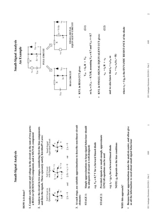
  • 1. Small-Signal Analysis Small-Signal Analysis An Example HOW is it done? 1. Consider each current and voltage in the circuit as the sum of two parts: R vin a BIAS (or QUIESCENT) component, and a SIGNAL component V D + vd VIN ID + id 2. Analyse the circuit in two stages, considering first the bias components and then the signals. These separately satisfy Kirchhoff’s Laws: FULL CIRCUIT Full Circuit in Full Circuit Small-Signal Quiescent state with Signals Equivalent Circuit I1 I2 + i2 I1 + i1 i1 I2 i2 R R rd = VT/ID I4 I4 + i4 i4 VIN vin vd I3 I3 + i3 i3 VD ID id  In = 0 and  (In + in ) = 0  in = 0 BIAS CIRCUIT SMALL-SIGNAL EQUIVALENT CIRCUIT 3. At each stage, use suitable approximations to describe non-linear circuit elements: • KVL in BIAS CCT gives: STAGE 1: Simple approximations to large-signal behaviour should VIN = ID R + VD (2.1) be adequate (if circuit is well-designed) so ID  (VIN - 0.7)/R, assuming VD  0.7 and VIN >> 0.7 e.g. VD  0.7 V for a forward biased diode • KVL in SMALL-SIGNAL EQUIVALENT CCT gives: STAGE 2: Provided signals are small enough, approximate LINEAR equations can be used vin = id R + vd (2.2) e.g. id = gdvd for a forward biased diode and we also know that id = vd/rd, so NOTE: gd depends on the bias conditions vd = vin rd/(rd + R) WHY this approach? where rd = 1/gd is the DYNAMIC RESISTANCE of the diode • Because linear approximations make the analysis easier, and often give us all the information we need about small signal behaviour EE1 Analogue Electronics 2010/2011 - Part 2 ASH 1 EE1 Analogue Electronics 2010/2011 - Part 2 ASH 2
  • 2. Small-Signal Equivalent Models Small-Signal Equivalent Models 2-Terminal Devices 2-Terminal Devices • Small-Signal Equivalent Circuit is formed by replacing each circuit element with its SMALL-SIGNAL EQUIVALENT MODEL (SSEM) Device Symbol Defining equations Small-signal equiv. model • The SSEM describes schematically the relationship between the signal voltages and currents at the device terminals DC voltage source V = const rd = dV/dI = 0 short-circuit • DYNAMIC RESISTANCE I = const DC current source For 2-Terminal devices where the I-V relationship depends only on the rd  open-circuit instantaneous values of I and V, the SSEM is a resistor with value rd, where: Resistor V=IR rd = [dV/dI]OP (2.3) R rd = R Here []OP indicates that the derivative is evaluated at the operating point Junction diode I = I0 exp(V/VT) (forward biased) rd = VT /I Examples: resistor (rd = R); diode at low frequency Capacitor Q=CV • DYNAMIC CAPACITANCE C cd = C For devices where the current depends on the rate of change of the voltage across the terminals, we can describe this dependence in terms NB Second order and high frequency effects neglected of a dynamic capacitance cd: cd = [dQ/dV]OP (2.4) This is similar to the usual capacitor equation (i.e. C = Q/V), except that we are now allowing the stored charge Q to be a non-linear function of the applied voltage Examples: capacitor (cd = C); diode at high freq (cd appears in parallel with rd) EE1 Analogue Electronics 2010/2011 - Part 2 ASH 3 EE1 Analogue Electronics 2010/2011 - Part 2 ASH 4
  • 3. Small-Signal BJT Model - 1 Small-Signal BJT Model - 2 (VCCS version, neglecting ro) (ICCS version, neglecting ro) • Need an SSEM to describe the relationship between the signals ib, ic, vbe • Often we will want to express ic in terms of ib, using a current-controlled and vce in active mode current source (ICCS): Given large-signal relationships: IC = IS exp(VBE/VT) ib ic B ib  ib C IB = IC / = (IS /) exp(VBE/VT) rbe • IB-VBE relationship is diode-like  Use a dynamic resistance to represent the base-emitter junction E ie • IC-VBE relationship is also diode-like, but now the voltage between B & E is controlling the current between C & E NB  here (also called hfe) is the slope of the IC-IB characteristic at the  Use a voltage-controlled current source (VCCS) to represent the operating point. Strictly we should distinguish this from the  used collector signal current: earlier in the large-signal equations. However, the difference is usually small, so we shall ignore it  SIMPLIFIED HYBRID- MODEL: • How are the parameters in the two models related? ib ic ib = vbe /rbe (2.5) Eliminating vbe from Equations 2.5 and 2.6 gives ic = gmrbeib, and we also B gmvbe C know that ic =  ib, so: vbe rbe ic = gm vbe (2.6)  = gm rbe (2.9) ie = ib + ic E ie • Some TYPICAL VALUES: For a BJT with  = 100, biased at IC = 1 mA: NOTE: rbe often referred to as r gm = IC /VT  40 mS • SMALL-SIGNAL PARAMETERS: rbe =  /gm  2.5 k rbe = [dVBE/dIB]OP = VT/IB (2.7) gm = [dIC/dVBE]OP = IC/VT (2.8) EE1 Analogue Electronics 2010/2011 - Part 2 ASH 5 EE1 Analogue Electronics 2010/2011 - Part 2 ASH 6
  • 4. Small-Signal BJT Model - 3 C-E Amplifier Revisited The Early Effect Quiescent Analysis • For a real transistor, IC does show some dependence on VCE: IC VCC VCC IC VBIAS = VCC RB2 _________ (RB1 + RB2 ) RC RC RB1 RB = (RB1 //RB2 ) VCE COUT RB VBE CIN incr VBE V IN VOUT RB2 VBIAS RE CE RE VCE 0 FULL CIRCUIT BIAS CIRCUIT -VA • All curves, when extrapolated, cross the VCE axis at roughly the same • CIN, COUT and CE open-circuit at DC  omit from bias CCT point (-VA, 0). VA is the EARLY VOLTAGE, which normally lies in the range 50 to 100 V • KVL on input side of bias CCT gives: • Equation 1.2 becomes: VBIAS = IB RB + VBE + IE RE IC = IS.exp(VBE/VT).(1 + VCE/VA) (2.10) VBE  0.7 V, IE = (1 + )IB • Finite slope of the IC-VCE curve represents a SMALL-SIGNAL  IE  (VBIAS - 0.7)/[RE + RB/(1 + )] (2.12) OUTPUT RESISTANCE ro: ro = [VCE/IC]OP  VA/IC (2.11) NOTE: IE now shows some dependence on  as a result of the finite source impedance of VBIAS. However, we can minimise this by making RB << (1 + )RE. • So SSEM becomes: B gmvbe C gm = IC /VT • As before: rbe IC =  IE vbe ro ro = VA /IC rbe =  /gm and the quiescent voltages at the transistor terminals are: E VE = IERE, VB  VE + 0.7, VC = VCC - RC IC EE1 Analogue Electronics 2010/2011 - Part 2 ASH 7 EE1 Analogue Electronics 2010/2011 - Part 2 ASH 8
  • 5. C-E Amplifier Revisited C-E Amplifier Revisited Small-Signal Analysis - 1 Small-Signal Analysis - 2 • Assume capacitors are so large that they are effectively short-circuit at Small-Signal response can be characterised by three parameters: signal frequencies: • VOLTAGE GAIN: VCC Av = - gm (RC//ro) (2.14) RC RB1 [since vout = -gmvbe(RC//ro), and vbe = vin ] O/P I/P COUT CIN Similar to Equn 1.10, except that we are now taking the finite output resistance of the transistor into account RB2 e.g. If VA = 100 V and IC = 1 mA, then ro = VA /IC = 100 K. In this case RE CE the voltage gain with RC = 10 K is reduced from 400 (assuming ro infinite) to 364 FULL CIRCUIT • INPUT RESISTANCE: Ri = (RB1//RB2//rbe) = (RB//rbe) (2.15) Ri tells us about the loading effect imposed by the amplifier on the input gmvbe CIN COUT signal source. Usually it is dominated by the transistor input resistance vbe rbe ro rbe RB1 RB2 RC vin vout • OUTPUT RESISTANCE: RE CE Ro = (RC//ro) (2.16) Ro is the source impedance associated with the amplifier’s output SMALL-SIGNAL EQUIVALENT CCT voltage Also of interest: gmvbe • CURRENT GAIN Ai, which is the ratio of the short-circuit output vbe rbe ro current to the input current. This can be deduced from Av, Ri and Ro: RB1 RB2 RC vin vout Ai = AvRi/Ro SSEC assuming Large Capacitors EE1 Analogue Electronics 2010/2011 - Part 2 ASH 9 EE1 Analogue Electronics 2010/2011 - Part 2 ASH 10
  • 6. Emitter Degeneration - 1 Emitter Degeneration - 2 • Overall Ri now given by: What happens if we leave out the bypass capacitor? Ri = RB//[rbe + (1 + ) RE] (2.19) VCC • and vout = - ibRC, so Av given by: RC RB1 Av = -  RC /[rbe + (1 + ) RE] (2.20) COUT IMPORTANT CASES: CIN AV  - gmRC as RE  0 vIN vOUT RB2 RE Av  -  RC /RE if (1 + )RE >> rbe (these are the results we obtained in Part 1) FULL CIRCUIT Summary of C-E Amplifier Parameters ib  ib C-E with Emitter Grounded C-E vbe ro Degeneration (and ro = ) rbe vin RB1 RB2 RC vout ie Ri RB//rbe (RB//[rbe + (1 + )RE]) ve RE Ro RC//ro RC SSEC assuming Large Capacitors -  RC _______________ Av - gm (RC//ro ) NB Things get messy if ro is included, so we’ll neglect it [rbe + (1 + )RE] • KVL on input side gives: vin = vbe + ve = ib rbe + ie RE RE provides negative or DEGENERATIVE FEEDBACK which: and ie = (1 + )ib • Reduces gain  vin = [rbe + (1 + ) RE] ib (2.18) • Improves linearity (only a fraction of the input voltage appears across the base-emitter junction) So, RE increases the apparent input resistance at the base of the transistor from rbe to [rbe + (1 + ) RE] • Improves the high-frequency performance of the amplifier EE1 Analogue Electronics 2010/2011 - Part 2 ASH 11 EE1 Analogue Electronics 2010/2011 - Part 2 ASH 12
  • 7. Amplifier Macromodels • Given Av, Ri and Ro, we can replace an entire amplifier by its Small- Signal Equivalent Model: Ro Input vin Ri Av vin ~ Output We call this a MACROMODEL, because it describes the external characteristics of the amplifier without providing detailed information about the circuit configuration • We can use the macromodel to determine how the amplifier will interact with other circuits at its input or output. e.g. Source Amplifier Load RS Ro vS ~ vin Ri Av vin ~ RL vL The observed voltage gain vL/vS is reduced by the potential dividers at the input and output, giving: vL/vS = [Ri /(Ri + RS)].Av.[RL /(RL + Ro)] (2.21) So, the IN-CIRCUIT GAIN DEPENDS ON THE SOURCE AND LOAD RESISTANCES! This is one of the reasons we are interested in Ri and Ro • Macromodels are extremely useful when it comes to analysing more complex circuits, because they allow us to reduce the number of circuit elements to a minimum EE1 Analogue Electronics 2010/2011 - Part 2 ASH 13 EE1 Analogue Electronics 2010/2011 - Part 2 ASH 14
  • 8. AC- and DC-Coupled Circuits - 1 AC- and DC-Coupled Circuits - 2 • DISCRETE CIRCUITS e.g. for amplifier on Page 11: • AC-coupling may be used to provide DC isolation between successive stages. In this case, each stage requires its own bias circuitry |vL/vS| This approach is often used in high-frequency applications, where there is no requirement for operation at signal frequencies near zero LOW-FREQ MID-BAND HIGH-FREQ • INTEGRATED CIRCUITS e.g. Operational Amplifiers • Stages inside chip are DC-COUPLED, so their bias conditions are CIN(RS + Ri ) = 1 interrelated NB LOG-LOG plot • Bias condition for entire circuit is established by external negative feedback COUT(Ro + RL) = 1 • DC-coupling gives extra flexibility of operation down to zero signal  frequency NB Graph assumes Av, Ri and Ro are constant throughout low-freq • AC-COUPLING - Effect on Frequency Response and mid-band  not directly applicable to bypassed C-E amplifier Source Amplifier Load • In this course we will consider only the MID-BAND, where the RS CIN Ro COUT vS ~ vin Ri Av vin ~ RL vL coupling capacitors are effectively short-circuit, and high-frequency ZS Zo effects can be ignored For a DC-Coupled circuit, the mid-band extends down to zero ZS = RS + 1/j CIN Zo = Ro + 1/j COUT frequency • Gain falls off at high frequency due to junction capacitances of • HIGH-PASS FILTERS at input and output transistors + parasitic effects. • Equation 2.21 becomes: vL/vS = [Ri /(Ri + ZS)].Av.[RL /(RL + Zo)] (2.22) Cont’d ... EE1 Analogue Electronics 2010/2011 - Part 2 ASH 15 EE1 Analogue Electronics 2010/2011 - Part 2 ASH 16
  • 9. ANALOGUE ELECTRONICS PROBLEMS 2 1. You are asked to analyse a circuit containing a BJT with a  of 200 and an Early voltage of 100 V. Bias analysis shows that the transistor is in active mode, and that the quiescent collector current is 2 mA. Draw a small-signal equivalent model of the device, and assign values to the parameters rbe, gm and ro. 2. (a) Calculate the collector bias current and the quiescent output voltage for the amplifier in Figure Q2. (b) Draw a small-signal equivalent circuit for the amplifier, and determine the small- signal parameters Ri (input resistance), Ro (output resistance) and Av (voltage gain). +5V 3 k 430 k O/P I/P  = 100 VA = 120 V Figure Q2 3. The figure below shows a common-emitter amplifier with a bypassed emitter resistor. The transistor has a  of 50 and an Early voltage of 100 V. Calculate the quiescent output voltage VOUT, and the small-signal voltage gain vout/vin for this circuit. You may assume that the bypass capacitor C is effectively short-circuit at signal frequencies. + 20 V 3.3 k VOUT + vout vin ~ 4V 1.1 k C EE1 Analogue Electronics 2010/2011 - Problems 2 ASH 1
  • 10. 4. (a) Calculate the quiescent collector current for the common-emitter amplifier in Figure Q4, and confirm that the transistor is biased roughly in the middle of the active region. (b) Draw a small-signal equivalent circuit of the amplifier, and determine the parameters Ri, Ro and Av, assuming the transistor has infinite small-signal output resistance. +20 V 10 k 330 k O/P I/P = 200 43 k 1.5 k Figure Q4 5. To achieve a higher voltage gain, two amplifier stages similar to the one in Question 4 are cascaded as shown below. Coupling capacitors are used to provide DC isolation between the signal source and the first stage, and between the two stages. C1 C2 Stage 1 Stage 2 vin ~ VOUT + vout Draw a small-signal equivalent circuit for the two-stage amplifier, in which each stage is represented by a macromodel. Hence calculate the overall small-signal voltage gain vout/vin, assuming the coupling capacitors are effectively short-circuit at signal frequencies. EE1 Analogue Electronics 2010/2011 - Problems 2 ASH 2
  • 11. 6. Derive an expression for the variation of vo/vi with frequency for the passive network in Figure Q6. Hence show that the cut-off frequency fc is given by 2fcC(R1 + R2) = 1. NOTE: fc is the frequency at which the low-freq and high-freq asymptotes of the frequency response meet. R1 C vi R2 vo Figure Q6 Using the above result, calculate the cut-off frequencies associated with the coupling capacitors in the amplifier of Question 5, assuming C1 = 47 nF and C2 = 220 nF. Hence sketch the variation of the overall voltage gain with frequency in the low-frequency and mid-band regions. 7. Show that the small-signal voltage gain of the amplifier below is given by: Av = - (gm - 1/RB).(RC//ro//RB) where gm and ro are the usual hybrid- parameters of the transistor. VS RC RB O/P I/P EE1 Analogue Electronics 2010/2011 - Problems 2 ASH 3
  • 12. Answers 1 rbe = 2.5 k, gm = 80 mS, ro = 50 k 2 (a) IC = 1 mA, VOUT = 2 V; (b) Ri = 2.49 k, Ro = 2.93 k, Av = -117 3 VOUT = 10.3 V, Av = -354 4 (a) IC = 0.946 mA; (b) Ri = 33.8 k, Ro = 10 k, Av = -6.52 5 Av = 32.8 6 fc = 100 Hz, 16.5 Hz for C1, C2 EE1 Analogue Electronics 2010/2011 - Problems 2 ASH 4