SlideShare uma empresa Scribd logo
1 de 7
Baixar para ler offline
1 | P a g e
COLLEGE OF ENGINEERING & TECHNOLOGY
Assignments on Basic Electronic
Chapter-1(Basic concepts)
1.The gain of a certain amplifier is 30dB.Express it numerically.
2.An amplifier has a current gain of 60dB and power gain of 50dB.Find its voltage gain.
3.Give an implementation of logic inverter .why it is called so?
4.Draw the spectrum of a periodic squrewave with proper lebels.
5.What is the a signal and system.Difference between analog signal and digital signal.
6.Find the frequencies f and ῳ of a sine wave signal with period of 1ms.
7.A signal of 100mV is fed to an amplifier which produces output 8.5 volts.Find its voltage gain in dB.
Chapter-2(OPAMP)
1.What is virtual ground concept and write the characteristics of
ideal OPAMP.
2.Draw the equivalent model of an ideal OPAMP.
3.Why feedback is used in case of practical OPAMP.
4.What is an operational amplifier?Explain.
5.Find the voltage gain for the fig shown.
6.Derive the relation between CMRR and output voltage.
7. Find the output of the circuit shown on the right side.
8.Find the output of the figure shown in the right
side.
9.For the figure below the reference dc voltage are +12 and -
12 volt and V=0v then find the output for 1v p-p ac input.
2 | P a g e
10.Find the values of the resistors so the the circuit provies o/p V0=2V1+V2-4V3 for the circuit shown
below.
11.For the circuit below if the gain is -10,then the value of R i
12.For the ckt determine the current through all resistors if input is 1v.
13.What are the advantage of instrumentation amplifier and also derive the o/p expression.
14.What is the o/p of an integrator and differentiator if a Step i/p is given.
3 | P a g e
15.Find the gain for the circuit below.
16.The current i0 is if vi is 1.5v.
Chapter-3(Basics of semiconductor and PN junction diodes)
1.What is the cause and effect of the depletion layer in a pn junction diode?
2.Write down four applications of diode.
3.Compare the PIVs of a halfwave rectifier and full wave rectifier.
4.Explain why an inductor and a capacitor can act as filtering components.
5.Implement 2-i/p NAND gate by diode,transistor and resistors.
6. PN junction made up of which material (Si,Ge,GaAs) will have highest thermal stability and why ?
7. Give atleast two examples of semiconductors which are used for LED. Also express why?
8.What is a clipper circuit explain with an example?
9.Define mobility and conductivity of an intrinsicsemiconductor.
10.A diode has a reverse saturation current of 5µA at 250
c for a reverse voltage of 20v.Calculate the
reverse resistance.
11.An ideal diode acts like a bistable switch,justify.
12.Explain how diodes are useful in Clamping operation.Draw negative clamping circuit.Find the
relation between the time constant of the circuit and time period of the input signal.What should be
the full discharge time,in terms of the time constant of the circuit,for the capacitor you have used.
13.Explain the diode resistances and load line.
4 | P a g e
14.Write the analytic equation for the current which describes both forward and reverse
characterstics of a diode.A silicon diode has a forward voltage drop of 1.2v for a forward dc current
of 100mA.It has a reverse current of 1µA for a reverse voltage of 10v.Claculate the bulk and reverse
resistance of the diode.Find the ac resistance at forward dc current of 25 mA.
15. Find the output.
16.Find the output.
17.Find the output.
18. Find the output.
5 | P a g e
19.Why Si is preffered over Ge and what are the advantage of semiconductor.
20.Find the output.
21. Two junction diodes (identical) are connected as shown in fig. Find current through and voltage
across diode D1 and D2 .Given Is=0.2µA,ȵ=1,VT=25mV,supply voltage=15V
22. Derive all the parameters of rectifiers.
23. A full wave bridge rectifier with a 120V rms sinusoidal input has a load resistor of 1KΩ .
i)If silicon didodes are applied,what is the d.c voltage available at the load ?
ii)Determine the required PIV rating of each diode.
iii)Find maximum current through each diode during conduction.
iv)What is the power rating for each diode.
24.In the voltage regulator circuit find the power dissipation in the Zener diode.
Chapter-4 (Transistor and Its biasing)
1.Why NPN is preferred over PNP.
2.Why transistor is called so.
3.What is an amplifier.
6 | P a g e
4.Why common collector configuration is also called emitter follower. And what is its use.
5.What are the needs of biasing? Write short note on biasing.
6.Define ICBO and ICEO. Derive an expression to find the relation between them.
7.Explain the operation of PNP transistor.
8.Explain base width modulation or Early effect.
9.Derive relation among all the current gains.
10.Draw the characteristics of CB and CE configuration.
11. What is the phase relation between all the three configurations.
12.For the circuit shown below Find IE and Rc.
13.Find IC,RC ? 14.Find Q point and VC?
14.Why CE is widely used.Explain.
15.Tabulate the i/p and o/p impendances of all the configurations.
16.Explain transistor as an Amplifier and Switch/Inverter.
7 | P a g e
17.Given VCEQ and ICQ are 12V and 2A respectively when beta is 60 find the value of base and collector
resistors.
18.For the FIG a and b ,find the Q point. Given beta=100
19.Find the collector if minority current ,current gain and base current in CB configuration are 0.2µA
0.9 and 5µA respectively.
20.Derive the general expression of stability factor and also find the stability factor value of FIG a
and b of Question no.18.
21.Why fixed bias is called so and comment on its stability.
22.What is over drive factor.
23.How can we find in which region transistor is operating.
Prepared by: Mr.Soumya ranjan panda
Email-srpandaie@cet.edu.in

Mais conteúdo relacionado

Mais procurados

Common emitter amplifier by YEASIN NEWAJ
Common emitter amplifier by YEASIN NEWAJCommon emitter amplifier by YEASIN NEWAJ
Common emitter amplifier by YEASIN NEWAJYeasinNewaj
 
Ec6401 ec ii university questions
Ec6401 ec ii university questionsEc6401 ec ii university questions
Ec6401 ec ii university questionsMahi C
 
Common Emitter circuit
Common Emitter circuitCommon Emitter circuit
Common Emitter circuitMahoneyKadir
 
Ac analysis of bjt and mosfet inverting amplifiers
Ac analysis of bjt and mosfet inverting amplifiersAc analysis of bjt and mosfet inverting amplifiers
Ac analysis of bjt and mosfet inverting amplifiersMahoneyKadir
 
Lab 7 diode with operational amplifiers by kehali b. haileselassie and kou
Lab 7  diode with operational amplifiers by kehali b. haileselassie and kouLab 7  diode with operational amplifiers by kehali b. haileselassie and kou
Lab 7 diode with operational amplifiers by kehali b. haileselassie and koukehali Haileselassie
 
Class 12th Solids and semiconductor devices part 3
Class 12th Solids and semiconductor devices part 3Class 12th Solids and semiconductor devices part 3
Class 12th Solids and semiconductor devices part 3Arpit Meena
 
Basic Electronics (Rectifiers) by Er. Swapnil Kaware
Basic Electronics (Rectifiers) by Er. Swapnil KawareBasic Electronics (Rectifiers) by Er. Swapnil Kaware
Basic Electronics (Rectifiers) by Er. Swapnil KawareProf. Swapnil V. Kaware
 
Operational Amplifiers Basic
Operational Amplifiers BasicOperational Amplifiers Basic
Operational Amplifiers Basicsahed dewan
 
5 experiment -_characteristics_of_bipolar_junction_transistors
5 experiment -_characteristics_of_bipolar_junction_transistors5 experiment -_characteristics_of_bipolar_junction_transistors
5 experiment -_characteristics_of_bipolar_junction_transistorsengrsabi
 
5. differential amplifier
5. differential amplifier5. differential amplifier
5. differential amplifierShahbazQamar2
 
Lab 8 bipolar junction transistor characterstics
Lab 8  bipolar junction transistor charactersticsLab 8  bipolar junction transistor characterstics
Lab 8 bipolar junction transistor charactersticskehali Haileselassie
 
16 s1 ee2002_ld_multi-stage_differential_amplifiers_v1.3
16 s1 ee2002_ld_multi-stage_differential_amplifiers_v1.316 s1 ee2002_ld_multi-stage_differential_amplifiers_v1.3
16 s1 ee2002_ld_multi-stage_differential_amplifiers_v1.3MahoneyKadir
 

Mais procurados (19)

Common emitter amplifier by YEASIN NEWAJ
Common emitter amplifier by YEASIN NEWAJCommon emitter amplifier by YEASIN NEWAJ
Common emitter amplifier by YEASIN NEWAJ
 
Ec6401 ec ii university questions
Ec6401 ec ii university questionsEc6401 ec ii university questions
Ec6401 ec ii university questions
 
Common Emitter circuit
Common Emitter circuitCommon Emitter circuit
Common Emitter circuit
 
Q bank chap3,4,5,6
Q bank  chap3,4,5,6Q bank  chap3,4,5,6
Q bank chap3,4,5,6
 
BJT AC Analisi 5
BJT AC Analisi 5 BJT AC Analisi 5
BJT AC Analisi 5
 
Ac analysis of bjt and mosfet inverting amplifiers
Ac analysis of bjt and mosfet inverting amplifiersAc analysis of bjt and mosfet inverting amplifiers
Ac analysis of bjt and mosfet inverting amplifiers
 
Lab 7 diode with operational amplifiers by kehali b. haileselassie and kou
Lab 7  diode with operational amplifiers by kehali b. haileselassie and kouLab 7  diode with operational amplifiers by kehali b. haileselassie and kou
Lab 7 diode with operational amplifiers by kehali b. haileselassie and kou
 
Class 12th Solids and semiconductor devices part 3
Class 12th Solids and semiconductor devices part 3Class 12th Solids and semiconductor devices part 3
Class 12th Solids and semiconductor devices part 3
 
EC8353 ELECTRONIC DEVICES AND CIRCUITS Unit 2
EC8353 ELECTRONIC DEVICES AND CIRCUITS Unit 2EC8353 ELECTRONIC DEVICES AND CIRCUITS Unit 2
EC8353 ELECTRONIC DEVICES AND CIRCUITS Unit 2
 
Ade manual final
Ade manual finalAde manual final
Ade manual final
 
Basic Electronics (Rectifiers) by Er. Swapnil Kaware
Basic Electronics (Rectifiers) by Er. Swapnil KawareBasic Electronics (Rectifiers) by Er. Swapnil Kaware
Basic Electronics (Rectifiers) by Er. Swapnil Kaware
 
Operational Amplifiers Basic
Operational Amplifiers BasicOperational Amplifiers Basic
Operational Amplifiers Basic
 
Basic Electronics by Er. Swapnil Kaware
Basic Electronics by Er. Swapnil KawareBasic Electronics by Er. Swapnil Kaware
Basic Electronics by Er. Swapnil Kaware
 
5 experiment -_characteristics_of_bipolar_junction_transistors
5 experiment -_characteristics_of_bipolar_junction_transistors5 experiment -_characteristics_of_bipolar_junction_transistors
5 experiment -_characteristics_of_bipolar_junction_transistors
 
5. differential amplifier
5. differential amplifier5. differential amplifier
5. differential amplifier
 
Lab 8 bipolar junction transistor characterstics
Lab 8  bipolar junction transistor charactersticsLab 8  bipolar junction transistor characterstics
Lab 8 bipolar junction transistor characterstics
 
16 s1 ee2002_ld_multi-stage_differential_amplifiers_v1.3
16 s1 ee2002_ld_multi-stage_differential_amplifiers_v1.316 s1 ee2002_ld_multi-stage_differential_amplifiers_v1.3
16 s1 ee2002_ld_multi-stage_differential_amplifiers_v1.3
 
Summing Amplifer
Summing AmpliferSumming Amplifer
Summing Amplifer
 
Eca unit i.ppt
Eca unit i.pptEca unit i.ppt
Eca unit i.ppt
 

Semelhante a Electronics assignments

Vlsi model question paper 1
Vlsi model question paper 1Vlsi model question paper 1
Vlsi model question paper 1PUSHPALATHAV1
 
Basics of electrical_and_electronics-2019-syllabus-ktustudents.in
Basics of electrical_and_electronics-2019-syllabus-ktustudents.inBasics of electrical_and_electronics-2019-syllabus-ktustudents.in
Basics of electrical_and_electronics-2019-syllabus-ktustudents.inSreepadam Padam
 
EC8351-Electronic Circuits-I study material.pdf
EC8351-Electronic Circuits-I study material.pdfEC8351-Electronic Circuits-I study material.pdf
EC8351-Electronic Circuits-I study material.pdfRajaSekaran923497
 
Analog and Digital Electronics Lab Manual
Analog and Digital Electronics Lab ManualAnalog and Digital Electronics Lab Manual
Analog and Digital Electronics Lab ManualChirag Shetty
 
Simulated Analysis of Resonant Frequency Converter Using Different Tank Circu...
Simulated Analysis of Resonant Frequency Converter Using Different Tank Circu...Simulated Analysis of Resonant Frequency Converter Using Different Tank Circu...
Simulated Analysis of Resonant Frequency Converter Using Different Tank Circu...IJERD Editor
 
Basic Electrical Engineering
Basic Electrical EngineeringBasic Electrical Engineering
Basic Electrical EngineeringMathankumar S
 
Lecture 06 transistorremodel
Lecture 06 transistorremodelLecture 06 transistorremodel
Lecture 06 transistorremodelIsmael Cayo Apaza
 
Lab 4 Report Switching Voltage Regulators
Lab 4 Report Switching Voltage Regulators Lab 4 Report Switching Voltage Regulators
Lab 4 Report Switching Voltage Regulators Katrina Little
 
20 questions cmos ckts
20 questions cmos ckts20 questions cmos ckts
20 questions cmos cktsDeepak Gour
 
Assignment 1 Description Marks out of Wtg() Due date .docx
Assignment 1  Description Marks out of Wtg() Due date .docxAssignment 1  Description Marks out of Wtg() Due date .docx
Assignment 1 Description Marks out of Wtg() Due date .docxfredharris32
 
EC8252 NOTES 3rd to 5th unit_compressed.pdf
EC8252 NOTES 3rd to 5th unit_compressed.pdfEC8252 NOTES 3rd to 5th unit_compressed.pdf
EC8252 NOTES 3rd to 5th unit_compressed.pdfkabileshsk2
 
Ec6412 linear-integrated-circuit-laboratory
Ec6412 linear-integrated-circuit-laboratoryEc6412 linear-integrated-circuit-laboratory
Ec6412 linear-integrated-circuit-laboratoryPRADEEPJ30
 
Cntl model paper
Cntl model paperCntl model paper
Cntl model papersce,bhopal
 
Simple 100 w inverter circuit
Simple 100 w inverter circuitSimple 100 w inverter circuit
Simple 100 w inverter circuitNarasimha Reddy
 
A novel voltage reference without the operational amplifier and resistors
A novel voltage reference without the operational amplifier and resistorsA novel voltage reference without the operational amplifier and resistors
A novel voltage reference without the operational amplifier and resistorsIJRES Journal
 

Semelhante a Electronics assignments (20)

Vlsi model question paper 1
Vlsi model question paper 1Vlsi model question paper 1
Vlsi model question paper 1
 
48096558 ec2258-lm
48096558 ec2258-lm48096558 ec2258-lm
48096558 ec2258-lm
 
ADC LAB MANUAL.docx
ADC LAB MANUAL.docxADC LAB MANUAL.docx
ADC LAB MANUAL.docx
 
Basics of electrical_and_electronics-2019-syllabus-ktustudents.in
Basics of electrical_and_electronics-2019-syllabus-ktustudents.inBasics of electrical_and_electronics-2019-syllabus-ktustudents.in
Basics of electrical_and_electronics-2019-syllabus-ktustudents.in
 
EC8351-Electronic Circuits-I study material.pdf
EC8351-Electronic Circuits-I study material.pdfEC8351-Electronic Circuits-I study material.pdf
EC8351-Electronic Circuits-I study material.pdf
 
Pdc lab manualnew
Pdc lab manualnewPdc lab manualnew
Pdc lab manualnew
 
Analog and Digital Electronics Lab Manual
Analog and Digital Electronics Lab ManualAnalog and Digital Electronics Lab Manual
Analog and Digital Electronics Lab Manual
 
PEQPAU.pdf
PEQPAU.pdfPEQPAU.pdf
PEQPAU.pdf
 
Simulated Analysis of Resonant Frequency Converter Using Different Tank Circu...
Simulated Analysis of Resonant Frequency Converter Using Different Tank Circu...Simulated Analysis of Resonant Frequency Converter Using Different Tank Circu...
Simulated Analysis of Resonant Frequency Converter Using Different Tank Circu...
 
Basic Electrical Engineering
Basic Electrical EngineeringBasic Electrical Engineering
Basic Electrical Engineering
 
Lecture 06 transistorremodel
Lecture 06 transistorremodelLecture 06 transistorremodel
Lecture 06 transistorremodel
 
Lab 4 Report Switching Voltage Regulators
Lab 4 Report Switching Voltage Regulators Lab 4 Report Switching Voltage Regulators
Lab 4 Report Switching Voltage Regulators
 
20 questions cmos ckts
20 questions cmos ckts20 questions cmos ckts
20 questions cmos ckts
 
Assignment 1 Description Marks out of Wtg() Due date .docx
Assignment 1  Description Marks out of Wtg() Due date .docxAssignment 1  Description Marks out of Wtg() Due date .docx
Assignment 1 Description Marks out of Wtg() Due date .docx
 
EC8252 NOTES 3rd to 5th unit_compressed.pdf
EC8252 NOTES 3rd to 5th unit_compressed.pdfEC8252 NOTES 3rd to 5th unit_compressed.pdf
EC8252 NOTES 3rd to 5th unit_compressed.pdf
 
Ec6412 linear-integrated-circuit-laboratory
Ec6412 linear-integrated-circuit-laboratoryEc6412 linear-integrated-circuit-laboratory
Ec6412 linear-integrated-circuit-laboratory
 
Cntl model paper
Cntl model paperCntl model paper
Cntl model paper
 
Test2
Test2Test2
Test2
 
Simple 100 w inverter circuit
Simple 100 w inverter circuitSimple 100 w inverter circuit
Simple 100 w inverter circuit
 
A novel voltage reference without the operational amplifier and resistors
A novel voltage reference without the operational amplifier and resistorsA novel voltage reference without the operational amplifier and resistors
A novel voltage reference without the operational amplifier and resistors
 

Electronics assignments

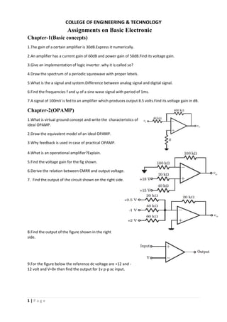
  • 1. 1 | P a g e COLLEGE OF ENGINEERING & TECHNOLOGY Assignments on Basic Electronic Chapter-1(Basic concepts) 1.The gain of a certain amplifier is 30dB.Express it numerically. 2.An amplifier has a current gain of 60dB and power gain of 50dB.Find its voltage gain. 3.Give an implementation of logic inverter .why it is called so? 4.Draw the spectrum of a periodic squrewave with proper lebels. 5.What is the a signal and system.Difference between analog signal and digital signal. 6.Find the frequencies f and ῳ of a sine wave signal with period of 1ms. 7.A signal of 100mV is fed to an amplifier which produces output 8.5 volts.Find its voltage gain in dB. Chapter-2(OPAMP) 1.What is virtual ground concept and write the characteristics of ideal OPAMP. 2.Draw the equivalent model of an ideal OPAMP. 3.Why feedback is used in case of practical OPAMP. 4.What is an operational amplifier?Explain. 5.Find the voltage gain for the fig shown. 6.Derive the relation between CMRR and output voltage. 7. Find the output of the circuit shown on the right side. 8.Find the output of the figure shown in the right side. 9.For the figure below the reference dc voltage are +12 and - 12 volt and V=0v then find the output for 1v p-p ac input.
  • 2. 2 | P a g e 10.Find the values of the resistors so the the circuit provies o/p V0=2V1+V2-4V3 for the circuit shown below. 11.For the circuit below if the gain is -10,then the value of R i 12.For the ckt determine the current through all resistors if input is 1v. 13.What are the advantage of instrumentation amplifier and also derive the o/p expression. 14.What is the o/p of an integrator and differentiator if a Step i/p is given.
  • 3. 3 | P a g e 15.Find the gain for the circuit below. 16.The current i0 is if vi is 1.5v. Chapter-3(Basics of semiconductor and PN junction diodes) 1.What is the cause and effect of the depletion layer in a pn junction diode? 2.Write down four applications of diode. 3.Compare the PIVs of a halfwave rectifier and full wave rectifier. 4.Explain why an inductor and a capacitor can act as filtering components. 5.Implement 2-i/p NAND gate by diode,transistor and resistors. 6. PN junction made up of which material (Si,Ge,GaAs) will have highest thermal stability and why ? 7. Give atleast two examples of semiconductors which are used for LED. Also express why? 8.What is a clipper circuit explain with an example? 9.Define mobility and conductivity of an intrinsicsemiconductor. 10.A diode has a reverse saturation current of 5µA at 250 c for a reverse voltage of 20v.Calculate the reverse resistance. 11.An ideal diode acts like a bistable switch,justify. 12.Explain how diodes are useful in Clamping operation.Draw negative clamping circuit.Find the relation between the time constant of the circuit and time period of the input signal.What should be the full discharge time,in terms of the time constant of the circuit,for the capacitor you have used. 13.Explain the diode resistances and load line.
  • 4. 4 | P a g e 14.Write the analytic equation for the current which describes both forward and reverse characterstics of a diode.A silicon diode has a forward voltage drop of 1.2v for a forward dc current of 100mA.It has a reverse current of 1µA for a reverse voltage of 10v.Claculate the bulk and reverse resistance of the diode.Find the ac resistance at forward dc current of 25 mA. 15. Find the output. 16.Find the output. 17.Find the output. 18. Find the output.
  • 5. 5 | P a g e 19.Why Si is preffered over Ge and what are the advantage of semiconductor. 20.Find the output. 21. Two junction diodes (identical) are connected as shown in fig. Find current through and voltage across diode D1 and D2 .Given Is=0.2µA,ȵ=1,VT=25mV,supply voltage=15V 22. Derive all the parameters of rectifiers. 23. A full wave bridge rectifier with a 120V rms sinusoidal input has a load resistor of 1KΩ . i)If silicon didodes are applied,what is the d.c voltage available at the load ? ii)Determine the required PIV rating of each diode. iii)Find maximum current through each diode during conduction. iv)What is the power rating for each diode. 24.In the voltage regulator circuit find the power dissipation in the Zener diode. Chapter-4 (Transistor and Its biasing) 1.Why NPN is preferred over PNP. 2.Why transistor is called so. 3.What is an amplifier.
  • 6. 6 | P a g e 4.Why common collector configuration is also called emitter follower. And what is its use. 5.What are the needs of biasing? Write short note on biasing. 6.Define ICBO and ICEO. Derive an expression to find the relation between them. 7.Explain the operation of PNP transistor. 8.Explain base width modulation or Early effect. 9.Derive relation among all the current gains. 10.Draw the characteristics of CB and CE configuration. 11. What is the phase relation between all the three configurations. 12.For the circuit shown below Find IE and Rc. 13.Find IC,RC ? 14.Find Q point and VC? 14.Why CE is widely used.Explain. 15.Tabulate the i/p and o/p impendances of all the configurations. 16.Explain transistor as an Amplifier and Switch/Inverter.
  • 7. 7 | P a g e 17.Given VCEQ and ICQ are 12V and 2A respectively when beta is 60 find the value of base and collector resistors. 18.For the FIG a and b ,find the Q point. Given beta=100 19.Find the collector if minority current ,current gain and base current in CB configuration are 0.2µA 0.9 and 5µA respectively. 20.Derive the general expression of stability factor and also find the stability factor value of FIG a and b of Question no.18. 21.Why fixed bias is called so and comment on its stability. 22.What is over drive factor. 23.How can we find in which region transistor is operating. Prepared by: Mr.Soumya ranjan panda Email-srpandaie@cet.edu.in