Apidays New York 2024 - Passkeys: Developing APIs to enable passwordless auth...
Merix Capabilities Ext Na 1 09
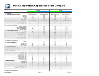
1. Merix Corporation Capabilities Cross Compare
San Jose Oregon
Volume Production Controlled Volume Production Volume Production Controlled Volume Production
Class A Class B Class A Class B
1.0 Material
1.1 Global Material Offerings All Sites Number of Conductive layers Number of Conductive layers Number of Conductive layer Number of Conductive layer
Isola FR406: 2 - 30 32 - 40 2 - 30 32 - 40
Isola 370HR: 2 - 30 32 – 40 2 - 30 32 – 40
ITEQ 180: NO 2 - 40 NO 2 - 40
FR408: 2 - 30 32 – 40 2 - 30 32 – 40
N4000-13 & 13SI: 2 - 30 32 - 40 2 - 30 32 - 40
Rogers 4350/4450: M/L & MIXED Dielectric M/L & MIXED Dielectric M/L & MIXED Dielectric M/L & MIXED Dielectric
1.2 Additional Standard Based Material
Standard FR4: 2 - 30 32 – 40 2 - 30 32 – 40
High Tg FR4 (Nelco-29): 2 - 30 32 – 40 2 - 30 32 – 40
High Tg Modified FR-4 (IS415) 2 - 30 32 – 40 2 - 30 32 – 40
1.3 Low Loss E-Glass Materials
High Freq. FR4 (FR408): 2 - 30 32 – 40 2 - 30 32 – 40
High Freq. Modified FR4 (IS620): 2 - 30 32 – 40 2 - 30 32 – 40
Polyclad GETEK & MEM Megtron: NO NO NO NO
Nelco 4000-13& 13SI: 2 - 30 32 – 40 2 - 30 32 – 40
1.4 Lead-Free Qualified Materials
ITEQ 180: NO 2 - 40 NO 2 - 40
High Tg CAF Resistant (370HR): 2 - 30 32 – 40 2 - 30 32 – 40
High Tg FR4 (Nelco-29): 2 - 30 32 – 40 2 - 30 32 – 40
High Tg Modified FR-4 (IS415) 2 - 30 32 – 40 2 - 30 32 – 40
Polyimide: 2 - 30 32 – 40 2 - 30 32 – 40
1.5 Lead-Free Low Loss Materials
High Freq. FR4 (FR408): 2 - 30 32 – 40 2 - 30 32 – 40
High Freq. Modified FR4 (IS620): 2 - 30 32 – 40 2 - 30 32 – 40
Nelco 4000-13EP and EPSI: 2 - 30 32 – 40 2 - 30 32 – 40
1.6 High Temperature Materials
Polyimide: 2 - 30 32 – 40 2 - 30 32 – 40
1.7 Commercial RF Materials
Roger 3000 Series: YES YES YES YES
Roger 4000 Series: YES YES YES YES
Taconic RF Materials: YES YES NO YES
1.8 Advanced RF Materials
Nelco 9000 Series (PTFE): 1-2 NO NO NO
Roger 6000 Series: 1–2 NO NO NO
Roger 5000 Series: 1–2 NO NO NO
1.9 Asia Material Offering
Isola 400,402, and ED130UV (Tg=125-145C): NO NO NO NO
Polyclad 370/ Turbo (Tg=175C): NO NO NO NO
ITEQ IT140(Tg=140C) NO NO NO NO
Nanya NP-140 (Tg=140C) NO NO NO NO
SHENGYI S1141 (Tg=135C): NO NO NO NO
SHENGYI S1441 (Tg=140C): NO NO NO NO
ITEQ IT158 (Tg=150C): NO NO NO NO
SHENGYI S1170 (Tg=170C): NO NO NO NO
ITEQ IT170 (Tg=170C) NO NO NO NO
1.10 Buried Capacitance
Isola FR406– 2mil YES YES YES YES
Isola FR408- 2mil YES YES YES YES
Isola 370HR-2 mil YES YES YES YES
Nelco-13 and -13Si – 2mil YES YES YES YES
Isola IS620 – 2mil YES YES YES YES
Polyimide P96 – 2mil YES YES YES YES
Oak-Mitsui Faradflex – BC 24 ( 1 mil) NO NO YES YES
Oak-Mitsui Faradflex – BC12TM (.5 mil) NO NO NO YES
1.11 Panel Sizes and Useable Area
Merix Corporation Page 1 of 5 Rev:090128
2. San Jose Oregon
Volume Production Controlled Volume Production Volume Production Controlled Volume Production
Class A Class B Class A Class B
18 X 24 18 X 24
Multilayer Panel Sizes: 12 X 18 16 X 18 21 X 24 16 x 18
Non Usable Border on Panel:
Double Sided Boards: .65 .65 .65 .55
Multilayer Boards: .75 .75 .65 .55
Spacing Between Boards: (Routing Process)
Double Sided and Multilayer Boards: .150 .100 .150 .100
2.0 Stack-ups
2.1 Overall Thickness Range and Tolerances
Overall Board Thickness: ≤ ≤ ≤ ≤
.126 - .240 .240 .126 - .240 .275
Overall Board Thickness Tolerance:
< .020”: +/- 15% +/- 15% +/- 15% +/- 15%
.031”: +/- 15% +/- 10% +/- 15% +/- 10%
.062”: +/- 10% +/- 8% +/- 10% +/- 8%
.093”: +/- 10% +/- 8% +/- 10% +/- 8%
.125”: +/- 10% +/- 8% +/- 10% +/- 8%
.187”: +/- 10% +/- 8% +/- 10% +/- 8%
2.2 Flatness Spec
Flatness: (Warp per Inch) .010 .007 .010 .0075
2.3 Thinnest Dielectric Finished
Thin Board Overall Thickness: .017 .013 .017 .015
Thinnest Plated Core: .012 .008 .012 .008
3.0 Mechanical Capabilities
3.1 Machining Drill Capabilities
Primary Drilled Hole Location Tolerance to Datum (Hole) Zero
(DTP): 0.007 0.006 0.007 0.006
2nd Drill Hole Location Tolerance to Datum Zero (DTP): 0.014 0.011 0.014 0.011
Minimum Clearance from Copper Conductor to Mechanical Drilled Hole: .0085 .008 .0085 .008
Minimum Clearance from Copper Conductor to a Laser Drilled Hole: .008 .006 .0085 .008
3.2 Plated Through Hole Capabilities
Smallest Plated Thru Hole Size: (Finished Via Size with Finished
Hole Size - 1 mil Min Ave Copper Requirement)
Finished Panel Thickness < .020”: .004 .003 .006 .006
Finished Panel Thickness .031”: .004 .004 .006 .006
Finished Panel Thickness.062”: .006 .006 .006 .006
Finished Panel Thickness.093”: .010 .008 .008 .008
Finished Panel Thickness.125”: .012 .008 .008 .008
Finished Panel Thickness.187”: .015 .012 .014 .012
Plated Hole Tolerance: +/-.003 +/-.002 +/- .003 +/- .002
Aspect Ratio (with 10 mil drill): 10:1 12:1 12.5:1 14:1
Plated Hole Spacing Minimum (Drilled hole to hole): .022 .015 .022 .015
3.3 Non Plated Through Holes
Smallest Non Plated Hole Size: (Finished) .010 .008 .010 .008
Largest Non-Plated Hole Size Routed: .200 NO LIMIT .200 NO LIMIT
Largest Primary Drilled and Tented Non-Plated Hole: .200 .250 .200 .250
Non-plated Routed Hole Tolerance: +/- .005 +/- .003 +/- .005 +/- .003
Minimum NPTH to Edge of Board Spacing: .020 .010 .020 .010
3.4 Micro Via (µVia) Capabilities
Smallest Laser µVia Hole Size: ( Via Size with 0.4 mil Copper
Requirement) .004 .004 .004 .004
Largest Drilled Laser Via: .010 .010 .006 > .009
Via Aspect Ratio 0.8:1 .9:1 .75:1 .85:1
Capture Pad Size: µvia + .010 µvia + .006 µvia + .010 µvia + .007
Landing Pad Size: µvia + .010 µvia + .006 µvia + .010 µvia + .007
Stacked Via NO 2 NO 3
Type I Capabilities YES YES YES YES
Type II Capabilities YES YES YES YES
Type III Capabilities NO NO NO YES
3.5 Control Depth Drill Capabilities
Smallest Control Depth Drill .008 .006 .010 .010
Largest Control Depth Drill .125 .257 .125 .125
Minimum Backside Dielectric Separation .008 .005 .007 .007
Control Depth Drill Depth Tolerance .005 .002 .005 .002
Control Depth Drill Aspect Ratio (with tolerance) .75:1 .85:1 .75:1 .85:1
3.6 Back Drilling Capabilities
Merix Corporation Page 2 of 5 Rev:090128
3. San Jose Oregon
Volume Production Controlled Volume Production Volume Production Controlled Volume Production
Class A Class B Class A Class B
Minimum Back Drill Drilled Diameter .022 .020 .022 .020
Drilled Hole Over Finished Hole Size .012 .010 .012 .010
Drill Depth Tolerance +/- .008 +/- .005 +/-.008 +/-.005
Number of Drilled Depths per Side MULTIPLE MULTIPLE MULTIPLE MULTIPLE
3.7 Scoring Capabilities
Angles: 60° 30° / 45° 30° 30°
Offset Tolerance: +/- .010 +/- .005 +/- .003 +/- .002
Optimum Remaining Web Thickness: .018 .012 .015 .012
Remaining Web Tolerance +/- .005 +/- .003 +/- .005 +/-.002
True Position Tolerance: .010 .005 .008 .005
3.8 Edge Connector Bevel Capabilities
Finger Tip Angle: 45° 30° / 20° 49°, 45°, 40° 30°, 20°
Bevel Depth Tolerance: +/- .010 +/- .005 +/- .008 +/- .005
3.9 Profile Capabilities
Standard Router Bit Diameter: .093 & .125 .062,.039,.031 1.6 mm, 2.4mm, .125 .031, 1mm
Routed Profile Tolerance: (18”X 24” Panel): +/- 0.005 +/- 0.004 +/- 0.005 +/- 0.004
Routed Cutout Tolerance: (0.50” x 0.50”): +/- 0.005 +/- 0.004 +/- 0.005 +/- 0.004
Minimum Internal Rout Radius: > .031 0.016 > .031 0.016
Minimum Routed Slot Width: > .062 .062 - .031 > .062 .062 - .031
4.0 Feature Size Capabilities
4.1 Innerlayer Capabilities
Minimum Conductor Width
Internal Starting Copper Weight ½ oz.: .00325 .003 .00325 .003
Internal Starting Copper Weight 1 oz.: .004 .0035 .004 .0035
Internal Starting Copper Weight 2 oz.: .006 .0055 .006 .0055
Internal Starting Copper Weight 3 oz: NO YES NO YES
Minimum Conductor Spacing: (Airgap)
Internal Starting Copper Weight ½ oz.: .0035 .00325 .0035 .00325
Internal Starting Copper Weight 1 oz.: .004 .004 .004 .004
Internal Starting Copper Weight 2 oz.: .006 .0055 .006 .0055
Internal Starting Copper Weight 3 oz.: NO YES NO YES
4.2 Outerlayer Capabilities (Finished Cu Thick)
(Finished Copper Thickness with Base Foil and Plating)
Minimum Conductor Width (Finished Copper Thickness with Base Foil and Plating)
External Copper Thickness 1.5 mil: .004 .003 .0035 .003
External Copper Thickness 2.0 mil: .0045 .0035 .004 .0035
External Copper Thickness 2.5 mil: .0055 .005 .0055 .005
External Copper Thickness 3.0 mil: .007 .006 .007 .006
(Finished Copper Thickness with Base Foil and Plating) (Finished Copper Thickness with Base Foil and Plating)
Minimum Conductor Spacing: (Airgap
External Copper Thickness 1.5 mil: .004 .003 .004 .0035
External Copper Thickness 2.0 mil: .0045 .0035 .0045 .004
External Copper Thickness 2.5 mil: .005 .004 .006 .0055
External Copper Thickness 3.0 mil: .007 .006 .007 .006
4.3 Pad Diameter to Finished Hole Size
Conventional Drilling:
Minimum Pad / Drill / Plated Hole:
(Pad Size for Tangency. Add 2X minimum annular ring as needed.) PAD / DRILL / HOLE PAD / DRILL / HOLE PAD / DRILL / HOLE PAD / DRILL / HOLE
.062 Thick Board: .020/.010/.006 .018/.008/.004 .020 / .010 / .006 .018 / .008 / .004
.093 Thick Board: .020 / .010 / .006 .019 / .010 / .006 .020 / .010 / .006 .019 / .010 / .006
.125 Thick Board ( .120 for HY only): .020 / .010 / .006 .019 / .010 / .006 .020 / .010 / .006 .019 / .010 / .006
.150 Thick Board: .022 / .012 / .008 .020 / .010 / .005 .022 / .012 / .008 .020 / .010 / .005
.187 Thick Board: .024 / .014 / .010 .022 / .012 / .008 .024 / .014 / .010 .022 / .012 / .008
Micro Drilling: Laser Via
Blind Via: .012/.006/.003 .010/.005/.003 .012/.004/.004 .011/.004/.004
Micro Drilling: Mechanical Via
Blind Via: .012/.006/.003 .010/.005/.003 .020 / .010 / .006 .019 / .008/ .004
5.0 Solder Mask and Silkscreen
5.1 Solder Mask
Minimum Solder Mask Clearance: (LPI)
Pad size larger than NPTH: .010 .006 .010 .006
Over Surface Image (pad relief): .006 .003 .005 .004
Web Between Surface Mount Pads: .004 .003 .003 .002
IPC SPEC COVERAGE IPC SPEC COVERAGE
Solder Mask Thickness Over Metal:
(SPC RANGES .0002 - .003 TYPICAL = .0007 over conductor) (SPC RANGES .0002 - .003 TYPICAL = .0007 over conductor)
BLUE, RED, BLACK, YELLOW,
Solder Mask Colors:
GREEN WHITE GREEN RED, BLUE, BLACK
Merix Corporation Page 3 of 5 Rev:090128
4. San Jose Oregon
Volume Production Controlled Volume Production Volume Production Controlled Volume Production
Class A Class B Class A Class B
Solder Mask Type: TAIYO-PSR4000 - HFX TAIYO-PSR4000 - HFX
Minimum Mask Defined Pad Diameter: .012 .010 .012 .010
Mask Defined Pad Minimum Overlap of Copper: .005 .0025 .005 .0025
5.2 Silkscreen
Minimum Width Silk Screen Image: .007 .005 .006 .005
Nomenclature Colors WHITE BLACK, YELLOW WHITE BLACK, YELLOW
6.0 Via-in-Pad - HDI
6.1 Epoxy Filled – Non Conductive
Epoxy Filled Thru Hole Capability: YES YES YES YES
Epoxy Filled Thru Hole Minimum: .010 .0072 .010 .008
Epoxy Filled Thru Hole Maximum: .018 .020 .020 .035
Epoxy Filled µVia Process: YES YES YES YES
Epoxy Filled µVia Hole Minimum: .0055 .004 .0055 .004
Minimum Board Thickness: .025 .020 .020 .020
Maximum Board Thickness: .125 .180 .120 .180
Via Fill Aspect Ratio: 8:1 12:1 10:1 12:1
Maximum Panel Size for µVia: 12 X 18 18 X 24 18 X 24 21 X 24
Outerlayer Trace Widths/Spacing .004 / .005 .0035 / .0045 .004 / .005 .004 / .0045 with Wrap Spec Class II
6.2 Copper Plated/ Filled
Copper Filled µVia Process: NO NO NO YES
Copper Filled µVia Hole Minimum: NO NO NO .004”
Copper Filled µVia Hole Maximum: NO NO NO .005”
Via Fill Aspect Ratio: NO NO NO .85:1
Maximum Board Thickness: NO NO NO <.150”
Outerlayer Trace Widths/Spacing: NO NO NO .004”/.004” with LB to Pattern
Combined with other fill technologies NO NO NO Must be reviewed
7.0 Military
7.1 Etch Back
2 Pt. Connection YES YES FR406, 370HR, FR408, Nelco-13, IS415, and Polyimide
3 Pt. Connection ( glass etch) YES YES FR406, 370HR and Polyimide
8.0 Cavity Boards - TMS
Through Rout Technology: NO YES YES YES
Step Rout Technology: NO YES YES YES
9.0 Thermal Management Technology
9.1 Coin Attached
Conductive Adhesive: NO NO YES YES
Solder Adhesive: NO NO NO YES
9.2 Pallet Attached
Conductive Adhesive: NO NO YES YES
Embedded Copper Technology(Merix Patent Pending): NO NO YES YES
10.0Surface Finishes Options
10.1 Surface Finishes Selection
Hot Air Solder Level: YES YES YES YES
Immersion Silver: Enthone Alpha Star MacDermid Sterling
Lead Free OSP : Shikoku F2(LX) Shikoku F2(LX)
Electroless Nickel Immersion Gold: YES YES YES YES
Immersion Tin: YES YES NO Yes – thru SJ
Full Body Gold: YES YES – 4 mil spacing on .5 oz YES YES
Bondable Gold: YES YES – 4 mil spacing on .5 oz NO NO
10.2 Mixed Finishes
Immersion Silver with Selective Hard Gold: YES YES YES YES
HASL with Selective Gold: YES YES YES YES
Dual Gold Plating: YES YES YES YES
Immersion Gold with OSP: YES YES NO NO
Immersion Gold with Selective Hard Gold: NO YES NO YES
Selective Hard Gold with OSP: YES YES YES YES
Recessed Fingers: YES YES NO NO
10.3 Lead-Free Surface Finishes
Immersion Silver: YES YES YES YES
Lead Free OSP : Enthone 106AX-HT Shikoku F2(LX)
Electroless Nickel Immersion Gold: YES YES YES YES
Immersion Tin: YES YES NO YES
Full Body Gold: YES YES YES YES
Lead-Free HASL: NO YES – Outside Service NO YES – Outside Service
11.0 Testing Capabilities
Merix Corporation Page 4 of 5 Rev:090128
5. San Jose Oregon
Volume Production Controlled Volume Production Volume Production Controlled Volume Production
Class A Class B Class A Class B
Minimum Test Continuity Resistance: 20 OHMS 10 OHMS 20 OHMS < 20 OHMS
Maximum Test Voltage: 100V 200V 100V 250V
Maximum Test Isolated Resistance: 10M OHMS 50M OHMS 10M OHMS 100M OHMS
Largest Test Bed Fixtured: 12 X 19.3 16.5 X 22.5 29.6 x 19.2 DD 29.6 x 19.2 DD
Largest Test Bed Flying Probe: 20 X 24 20 X 24 24X27 24X27
Electrical Test Pitch (Fixture Test): 0.019 0.016 .020 .016
Electrical Test Pitch (Flying Probe Test): 0.008 0.004 .010 .005
DC Line Resistance Testing: NO YES NO YES
Prop Delay: NO NO YES YES
12.0 Electrical Performance
TDR Test Tolerance (Print and Etch): +/- 10% +/- 7.5% +/- 10% +/- 7.5%
TDR Test Tolerance (Plated Copper): +/- 15% +/- 10% +/- 10% +/- 10%
TDR Test Tolerance Differential Measurements: +/- 15% +/- 10% +/- 10% +/- 10%
TDR Tolerance Single Ended Tolerance: +/- 10% +/- 7.5% +/- 10% +/- 10%
HiPot Testing (AC & DC): NO YES YES YES
13.0 Data & Documentation
13.1 Tooling Formats
Film Data Formats: ODB++ RS-274X ODB++ RS-274X
Drill Data Formats: ODB++ NC DATA & GERBER ODB++ NC DATA & GERBER
Route Data Formats: ODB++ NC DATA & GERBER ODB++ NC DATA & GERBER
Electrical Test Formats: ODB++ IPC-D-356A ODB++ IPC-D-356A
IPC-D-356A OR MENTOR NEUTRAL IPC-D-356A OR MENTOR NEUTRAL
Netlist Compare Formats: FILE FILE
ODB++ ODB++
13.2 Tooling Communication
Media Types & Data Transfer: FTP FTP
ftp.sj.merix.com ftp.merix.com
E-mail E-mail
cam@sj.merix.com cam@fg.merix.com
Compression Formats: ZIP, TAR, TGZ RAR, ARC ZIP, TAR, TGZ RAR, ARC
Secured Transfer: FTP PGP ENCRYPTION FTP PGP ENCRYPTION
Merix – San Jose Merix – Oregon
355 Turtle Creek Court 1521 Poplar Avenue
San Jose, California 95125 Forest Grove, Oregon 97116
Phone: (800) 800-3278 Phone: (888) 256-3749
Direct: (408) 280-0422 Direct: (503) 359-9300
FTP: ftp.sj.merix.com FTP: ftp.merix.com
Merix Corporation Page 5 of 5 Rev:090128