SlideShare uma empresa Scribd logo
1 de 9
Baixar para ler offline
EE-203
                               Diode Circuits Analysis
Problem 1:

Plot the load line and find the Q-point for the diode circuit in Figure 1 if V = 5 V and R =
10 kΩ. Use the i-v characteristic in Figure 2.


                                          Figure 1


                                          Figure 2


Solution:

5 = 104 I D + VD | VD = 0 I D = 0.500mA | I D = 0 VD = 5V
                                   4.5V
Forward biased - VD = 0.5V ID =          = 0.450 mA
                                   104 Ω


                                             1
EE-203
                                 Diode Circuits Analysis

                                   iD
                           2 mA


                          1 mA

                                            Q-point
                                                                      vD


                                        1        2        3   4   5


Problem 2:

Find the Q-point for the circuit in Figure 3 using the ideal diode model and constant
voltage drop model with Von=0.6V.


                                               Figure 3


Solution :

 Ideal diode model: ID = 1V/10kΩ = 100 µA; (100 µA, 0 V)
 Constant voltage drop model: ID = (1-0.6)V/10kΩ = 40.0 µA; (40.0 µA, 0.6 V)


                                                      2
EE-203
                                 Diode Circuits Analysis
Problem 3:

Find the Q-point for the diode in Figure 4 using (a) the ideal diode model and (b) the
constant voltage drop model with Von = 0.6 V. (c) Discuss the results. Which answer do
you feel is most correct?


                                                Figure 4


Solution :

Using Thévenin equivalent circuits yields and then combining the sources


                                     I                                    I
               1.2 k Ω                   1k Ω                                 2.2 k Ω
                         -   V   +                            -   V   +
         +                                       +                                      +
 1.6 V                                                   2V                                 0.4 V
         -                                       -                                      -


 (a) Ideal diode model: The 0.4 V source appears to be forward biasing the diode so
 we will assume it is "on". Substituting the ideal diode model for the forward region
              0.4V
 yields I =         = 0.182 mA . This current is greater than zero, which is consistent
             2.2k Ω
 with the diode being "on". Thus the Q-pt is (0 V, +0.182 mA).


                                                     3
EE-203
                             Diode Circuits Analysis
                                             I

                                    -        V   +             2.2 k Ω

                                                                         +
                                                                                 0.4 V
                                                                         -


              Ideal Diode:                                                               CVD:
                                         V
                                         on
                                  - +
                                                 I
                                 0.6 V                     2.2 k Ω

                                                                     +
                                                                         0.4 V
                                                                     -


(b) CVD model: The 0.4 V source appears to be forward biasing the diode so we will
assume it is "on". Substituting the CVD model with Von = 0.6 V yields
     0.4V − 0.6V
 I=              = −90.9 µ A . This current is negative which is not consistent with
        2.2k Ω
the assumption that the diode is "on". Thus the diode must be off. The resulting Q-pt
is: (0.4 V, 0 mA).

                             -     V +           I=0       2.2 k Ω

                                                                     +
                                                                         0.4 V
                                                                     -


(c) The second estimate is more realistic. 0.4 V is not sufficient to forward bias the
diode into significant conduction. For example, let us assume that IS = 10-15 A and
assume that the full 0.4 V appears across the diode. Then

                        ⎡    ⎛ 0.4V ⎞ ⎤
           iD = 10−15 A ⎢exp ⎜         − 1 = 8.89 nA , a very small current.
                        ⎣    ⎝ 0.025V ⎟ ⎥
                                      ⎠ ⎦


                                                       4
EE-203
                               Diode Circuits Analysis
Problem 4:

(a) Find I and V in the four circuits in Figure 5 using the ideal diode model. (b) Repeat
using the constant voltage drop model with Von = 0.7 V.


                                           Figure 5


 (a)
                                                              5 − ( −5)
        (a ) Diode is forward biased:V = − 5+0= − 5 V | I=              = 0.500 mA
                                                               20k Ω
        (b) Diode is reverse biased: I =0 | V=7 − 20k Ω ( I ) = 7 V | VD = −10 V
                                                        3 − ( −7)
        (c) Diode is forward biased:V =3 − 0=3 V | I=               = 0.500 mA
                                                          20k Ω
        (d ) Diode is reverse biased: I =0 | V= − 5 + 20k Ω ( I ) = −5 V | VD = −10 V
 (b)
                                                                 5 − ( −4.3)
       (a ) Diode is forward biased:V = − 5+0.7= − 4.3 V | I=                = 0.465 mA
                                                                   20k Ω
       (b) Diode is reverse biased: I =0 | V=7 − 20k Ω ( I ) = 7 V | VD = −10 V
                                                             2.3 − ( −7)
       (c) Diode is forward biased:V =3 − 0.7=2.3 V | I=                 = 0.465 mA
                                                                20k Ω
       (d ) Diode is reverse biased: I =0 | V= − 5 + 20k Ω ( I ) = −5 V | VD = −10 V


                                              5
EE-203
                                 Diode Circuits Analysis


Problem 5:

(a) Find I and V in the four circuits in Figure 5 using the ideal diode model if the resistor
values are changed to 100 kΩ. (b) Repeat using the constant voltage drop model with
Von = 0.6 V.

Solution :


(a)
                                                           5 − ( −5)
        (a ) Diode is forward biased:V = − 5+0= − 5 V | I=            = 100 µ A
                                                           100k Ω
        (b) Diode is reverse biased: I =0 A | V=7 − 100k Ω ( I ) = 7 V | VD = −10 V
                                                         3 − ( −7 )
        (c) Diode is forward biased:V =3 − 0=3 V | I=               = 100 µ A
                                                         100k Ω
        (d ) Diode is reverse biased: I =0 A | V= − 5 + 100k Ω ( I ) = −5 V | VD = −10 V
  (b)
                                                                   5 − ( −4.4)
         (a ) Diode is forward biased:V = − 5+0.6= − 4.4 V | I=                = 94.0 µ A
                                                                    100k Ω
         (b) Diode is reverse biased: I =0 | V=7 − 100k Ω ( I ) = 7 V | VD = −10 V
                                                               2.4 − ( −7)
         (c) Diode is forward biased:V =3 − 0.6=2.4 V | I=                 = 94.0 µ A
                                                                 100k Ω
         (d ) Diode is reverse biased: I =0 | V= − 5 + 20k Ω ( I ) = −5 V | VD = −10 V


                                                6
EE-203
                                Diode Circuits Analysis
Problem 6:

Find the Q-points for the diodes in the circuits in Figure 6 using the ideal diode model.


                                                    Figure 6


Solution :
 Diodes are labeled from left to right
                                                   10 − 0
  (a ) D1 on, D 2 off, D3 on: ID2 = 0 | ID1 =                = 1mA
                                                3k Ω + 7 k Ω
                0 − ( −5)
  I D3 + 1.00mA =         → I D3 = 1.00mA | VD2 = 5 − (10 − 3000 I D1 ) = −2V
                 2.5k Ω
  D1:(1.00 mA, 0 V ) D 2 :( 0 mA, − 2 V ) D3:(1.00 mA, 0 V )

  (b) D1 on, D 2 off, D3 off: I D2 = 0 | I D3 = 0
              10 − ( −5)
  I D1 =                        = 0.500mA | VD2 = 5 − (10 − 8000 I D1 ) = −1.00V
       8k Ω + 10k Ω + 12k Ω
  VD3 = − ( −5 + 12000 I D1 ) = −1.00V
  D1 : ( 0.500 mA, 0 V ) D2 : ( 0 A, − 1.00 V ) D3 : ( 0 A, − 1.00 V )


                                                7
EE-203
                                  Diode Circuits Analysis
  (c) D1 on, D 2 on, D3 on
         0 − ( −10)                          0 − ( 2)
  I D1 =            = 1.25mA > 0 | I10K =             = −0.200mA | I D 2 = I D1 + I10 K = 1.05mA > 0
            8k Ω                             10k Ω
          2 − ( −5)
  I12K =            = 0.583mA | I D 3 = I12 K − I10 K = 0.783mA > 0
           12k Ω
  D1 : (1.25 mA, 0 V ) D2 : (1.05 mA, 0 V ) D3 : ( 0.783 mA, 0 V )


  (d ) D1 off , D2 off , D3 on: I D1 = 0, I D 2 = 0
       12 − ( −5) V
  I D3 =              = 567µ A > 0 | VD1 = 0 − ( −5 + 10000 I D 3 ) = −0.667V < 0
           30     kΩ
  VD2 = 5 − (12 − 10000 I D 3 ) = −1.33V < 0
  D1 : ( 0 A, − 0.667 V ) D2 : ( 0 A, − 1.33 V ) D3 : ( 567 µ A, 0 V )


Problem 7:

Find the Q-points for the diodes in the circuits in Figure 6 using the constant voltage drop
model with Von = 0.6 V.

Solution:
 Diodes are labeled from left to right
                                                  10 − 0.6 − ( −0.6)
  (a ) D1 on, D 2 off, D3 on: ID2 = 0 | ID1 =                        = 1.00mA
                                                    3k Ω + 7 k Ω
                −0.6 − ( −5)
  I D3 + 1.00mA =            → I D3 = 0.760mA | VD2 = 5 − (10 − 0.6 − 3000 I D1 ) = −1.40V
                   2.5k Ω
  D1:(1.00 mA, 0.600 V ) D 2 :( 0 mA, − 1.40 V ) D3 :( 0.760 mA, 0.600V )

  (b) D1 on, D 2 off, D3 off: I D2 = 0 | I D3 = 0
           10 − 0.6 − ( −5)
  I D1 =                        = 0.480mA | VD2 = 5 − (10 − 0.6 − 8000 I D1 ) = −0.560V
       8k Ω + 10k Ω + 12k Ω
  VD3 = − ( −5 + 12000 I D1 ) = −0.760V
  D1:( 0.480 mA, 0.600 V ) D 2 :( 0 A, − 0.560 V ) D3:( 0 A, − 0.760 V )


                                                  8
EE-203
                                Diode Circuits Analysis
(c) D1 on, D 2 on, D3 on
        −0.6 − ( −9.4) V                             −0.6 − (1.4) V
I D1 =                      = 1.10mA > 0 | I10 K =                   = −0.200mA
               8         kΩ                              10       kΩ
                                             1.4 − ( −5) V
I D 2 = I D1 + I10 K = 0.900mA > 0 | I12 K =                 = 0.533mA | I D 3 = I12 K − I10 K = 0.733mA > 0
                                                 12      kΩ
D1:(1.10 mA, 0.600 V ) D 2 :( 0.900 mA, 0.600 V ) D3 :( 0.733 mA, 0.600 V)

(d ) D1 off , D2 off , D3 on: I D1 = 0, I D 2 = 0
     11.4 − ( −5) V
I D3 =                = 547 µ A > 0 | VD1 = 0 − ( −5 + 10000 I D 3 ) = −0.467V < 0
          30      kΩ
VD2 = 5 − (11.4 − 10000 I D 3 ) = −0.933V < 0
D1 : ( 0 A, − 0.467 V ) D2 : ( 0 A, − 0.933 V ) D3 : ( 547 µ A, 0 V )


                                                9

Mais conteúdo relacionado

Mais procurados

Diodes
DiodesDiodes
Diodescallr
 
Special purpose diodes
Special purpose diodesSpecial purpose diodes
Special purpose diodesadnanqayum
 
Rectifiers (ac dc)
Rectifiers (ac dc) Rectifiers (ac dc)
Rectifiers (ac dc) Taimur Ijaz
 
Solution manual for introduction to electric circuits
Solution manual for introduction to electric circuitsSolution manual for introduction to electric circuits
Solution manual for introduction to electric circuitschristian bastidas
 
Transistor as a switch
Transistor as a switchTransistor as a switch
Transistor as a switchOmed Diyari
 
Full wave bridge rectifier
Full wave bridge rectifierFull wave bridge rectifier
Full wave bridge rectifierRubel Biswas
 
VI CHARACTERISTICS OF PN JUNCTION DIODE IN हिंदी|PN JUNCTION DIODE|FORWARD & ...
VI CHARACTERISTICS OF PN JUNCTION DIODE IN हिंदी|PN JUNCTION DIODE|FORWARD & ...VI CHARACTERISTICS OF PN JUNCTION DIODE IN हिंदी|PN JUNCTION DIODE|FORWARD & ...
VI CHARACTERISTICS OF PN JUNCTION DIODE IN हिंदी|PN JUNCTION DIODE|FORWARD & ...Prasant Kumar
 
Clippers and clampers
Clippers and clampersClippers and clampers
Clippers and clamperstaranjeet10
 
I v characteristics of zener diode
I v characteristics of zener diodeI v characteristics of zener diode
I v characteristics of zener diodeMd. Mujahiduzzaman
 
Superposition theorem
Superposition theoremSuperposition theorem
Superposition theoremyash patel
 
Diodes and Its Application
Diodes and Its ApplicationDiodes and Its Application
Diodes and Its ApplicationJess Rangcasajo
 
Ac circuits notes
Ac circuits   notesAc circuits   notes
Ac circuits notesmadhu1729
 

Mais procurados (20)

Diodes
DiodesDiodes
Diodes
 
Special purpose diodes
Special purpose diodesSpecial purpose diodes
Special purpose diodes
 
Rectifiers (ac dc)
Rectifiers (ac dc) Rectifiers (ac dc)
Rectifiers (ac dc)
 
P n junction--eema
P n junction--eemaP n junction--eema
P n junction--eema
 
Solution manual for introduction to electric circuits
Solution manual for introduction to electric circuitsSolution manual for introduction to electric circuits
Solution manual for introduction to electric circuits
 
Ch02
Ch02Ch02
Ch02
 
Transistor as a switch
Transistor as a switchTransistor as a switch
Transistor as a switch
 
Full wave bridge rectifier
Full wave bridge rectifierFull wave bridge rectifier
Full wave bridge rectifier
 
VI CHARACTERISTICS OF PN JUNCTION DIODE IN हिंदी|PN JUNCTION DIODE|FORWARD & ...
VI CHARACTERISTICS OF PN JUNCTION DIODE IN हिंदी|PN JUNCTION DIODE|FORWARD & ...VI CHARACTERISTICS OF PN JUNCTION DIODE IN हिंदी|PN JUNCTION DIODE|FORWARD & ...
VI CHARACTERISTICS OF PN JUNCTION DIODE IN हिंदी|PN JUNCTION DIODE|FORWARD & ...
 
Diode circuits
Diode circuitsDiode circuits
Diode circuits
 
Clippers and clampers
Clippers and clampersClippers and clampers
Clippers and clampers
 
Pn junction
Pn junctionPn junction
Pn junction
 
I v characteristics of zener diode
I v characteristics of zener diodeI v characteristics of zener diode
I v characteristics of zener diode
 
Superposition theorem
Superposition theoremSuperposition theorem
Superposition theorem
 
IIT JEE Physics 1995
IIT JEE Physics   1995IIT JEE Physics   1995
IIT JEE Physics 1995
 
Diodes and Its Application
Diodes and Its ApplicationDiodes and Its Application
Diodes and Its Application
 
2 mesh analysis
2  mesh analysis2  mesh analysis
2 mesh analysis
 
Ac circuits notes
Ac circuits   notesAc circuits   notes
Ac circuits notes
 
Folded cascode1
Folded cascode1Folded cascode1
Folded cascode1
 
Source transformation
Source transformationSource transformation
Source transformation
 

Destaque (20)

Lecture 4 ver2 diode_app
Lecture 4 ver2 diode_appLecture 4 ver2 diode_app
Lecture 4 ver2 diode_app
 
Lecture5 diode circuits (1)
Lecture5 diode circuits (1)Lecture5 diode circuits (1)
Lecture5 diode circuits (1)
 
2 diode applications
2 diode applications2 diode applications
2 diode applications
 
Presentation on half and full wave ractifier.ppt
Presentation on half and full wave ractifier.pptPresentation on half and full wave ractifier.ppt
Presentation on half and full wave ractifier.ppt
 
EEE201 LECTURE 3~www.fida.com.bd
EEE201  LECTURE 3~www.fida.com.bdEEE201  LECTURE 3~www.fida.com.bd
EEE201 LECTURE 3~www.fida.com.bd
 
Clipper circuits
Clipper circuitsClipper circuits
Clipper circuits
 
Application of diode
Application of diodeApplication of diode
Application of diode
 
questions on diode analysis: Assignment6
questions on diode analysis: Assignment6questions on diode analysis: Assignment6
questions on diode analysis: Assignment6
 
C hapter 2 diode applications
C hapter 2 diode applicationsC hapter 2 diode applications
C hapter 2 diode applications
 
Basic electronics Tutorial 2 Solution
Basic electronics Tutorial 2 SolutionBasic electronics Tutorial 2 Solution
Basic electronics Tutorial 2 Solution
 
Basic electronics Tutorial 3
Basic electronics Tutorial 3Basic electronics Tutorial 3
Basic electronics Tutorial 3
 
Basic electronics Tutorial 1
Basic electronics Tutorial 1Basic electronics Tutorial 1
Basic electronics Tutorial 1
 
Basic electronics Tutorial 2
Basic electronics Tutorial 2Basic electronics Tutorial 2
Basic electronics Tutorial 2
 
Basic Electronics Tutorial 1 Solution
Basic Electronics Tutorial 1 SolutionBasic Electronics Tutorial 1 Solution
Basic Electronics Tutorial 1 Solution
 
Basic Electronics Tutorial 3 Solution
Basic Electronics Tutorial 3 SolutionBasic Electronics Tutorial 3 Solution
Basic Electronics Tutorial 3 Solution
 
Clipper circuit
Clipper circuitClipper circuit
Clipper circuit
 
Tanya makkar (5003)
Tanya makkar (5003)Tanya makkar (5003)
Tanya makkar (5003)
 
Chapter 1 electro mecha device part 4
Chapter 1 electro mecha device part 4Chapter 1 electro mecha device part 4
Chapter 1 electro mecha device part 4
 
Diode
DiodeDiode
Diode
 
Whip antenna
Whip antennaWhip antenna
Whip antenna
 

Semelhante a Diode circuits-analysis

Analog electronic circuit
Analog electronic circuitAnalog electronic circuit
Analog electronic circuitmohamed albanna
 
Et1 practical final examination
Et1 practical final examinationEt1 practical final examination
Et1 practical final examinationcheekeong1231
 
JUNCTION DIODE APPLICATIONS
JUNCTION DIODE APPLICATIONSJUNCTION DIODE APPLICATIONS
JUNCTION DIODE APPLICATIONSAsmita Bhagdikar
 
Diode by hashir ahmed
Diode by hashir ahmedDiode by hashir ahmed
Diode by hashir ahmedsyed Ahmed
 
01.pptx
01.pptx01.pptx
01.pptxTinNi9
 
lesson_4_1_semiconductor_physics-diode_and_transistors.ppt
lesson_4_1_semiconductor_physics-diode_and_transistors.pptlesson_4_1_semiconductor_physics-diode_and_transistors.ppt
lesson_4_1_semiconductor_physics-diode_and_transistors.pptKishore589011
 
Electronics 1 : Chapter # 04 : Diode Applications and Types
Electronics 1 : Chapter # 04 : Diode Applications and TypesElectronics 1 : Chapter # 04 : Diode Applications and Types
Electronics 1 : Chapter # 04 : Diode Applications and TypesSk_Group
 
BEF 12403 - Week 12 - Nodal Analysis Method.ppt
BEF 12403 - Week 12 - Nodal Analysis Method.pptBEF 12403 - Week 12 - Nodal Analysis Method.ppt
BEF 12403 - Week 12 - Nodal Analysis Method.pptLiewChiaPing
 
Chapter 1 techniques of dc circuit analysis
Chapter 1 techniques of dc circuit analysisChapter 1 techniques of dc circuit analysis
Chapter 1 techniques of dc circuit analysisAmirul Faiz Amil Azman
 
Voltage divider bias circuit | Dept of ECE | ANITS
Voltage divider bias circuit | Dept of ECE | ANITSVoltage divider bias circuit | Dept of ECE | ANITS
Voltage divider bias circuit | Dept of ECE | ANITSANILPRASAD58
 

Semelhante a Diode circuits-analysis (20)

Lec 15.pptx
Lec 15.pptxLec 15.pptx
Lec 15.pptx
 
3 nodal analysis
3 nodal analysis3 nodal analysis
3 nodal analysis
 
Analog electronic circuit
Analog electronic circuitAnalog electronic circuit
Analog electronic circuit
 
03
0303
03
 
Lab - 03
Lab - 03Lab - 03
Lab - 03
 
Lec 06 (2017).pdf
Lec 06 (2017).pdfLec 06 (2017).pdf
Lec 06 (2017).pdf
 
Et1 practical final examination
Et1 practical final examinationEt1 practical final examination
Et1 practical final examination
 
JUNCTION DIODE APPLICATIONS
JUNCTION DIODE APPLICATIONSJUNCTION DIODE APPLICATIONS
JUNCTION DIODE APPLICATIONS
 
Diode by hashir ahmed
Diode by hashir ahmedDiode by hashir ahmed
Diode by hashir ahmed
 
01.pptx
01.pptx01.pptx
01.pptx
 
Circuits5
Circuits5Circuits5
Circuits5
 
lesson_4_1_semiconductor_physics-diode_and_transistors.ppt
lesson_4_1_semiconductor_physics-diode_and_transistors.pptlesson_4_1_semiconductor_physics-diode_and_transistors.ppt
lesson_4_1_semiconductor_physics-diode_and_transistors.ppt
 
Electronics 1 : Chapter # 04 : Diode Applications and Types
Electronics 1 : Chapter # 04 : Diode Applications and TypesElectronics 1 : Chapter # 04 : Diode Applications and Types
Electronics 1 : Chapter # 04 : Diode Applications and Types
 
Diode logic crkts
Diode logic crktsDiode logic crkts
Diode logic crkts
 
Diode logic crkts
Diode logic crktsDiode logic crkts
Diode logic crkts
 
Diode
DiodeDiode
Diode
 
Lec 14.pdf
Lec 14.pdfLec 14.pdf
Lec 14.pdf
 
BEF 12403 - Week 12 - Nodal Analysis Method.ppt
BEF 12403 - Week 12 - Nodal Analysis Method.pptBEF 12403 - Week 12 - Nodal Analysis Method.ppt
BEF 12403 - Week 12 - Nodal Analysis Method.ppt
 
Chapter 1 techniques of dc circuit analysis
Chapter 1 techniques of dc circuit analysisChapter 1 techniques of dc circuit analysis
Chapter 1 techniques of dc circuit analysis
 
Voltage divider bias circuit | Dept of ECE | ANITS
Voltage divider bias circuit | Dept of ECE | ANITSVoltage divider bias circuit | Dept of ECE | ANITS
Voltage divider bias circuit | Dept of ECE | ANITS
 

Diode circuits-analysis

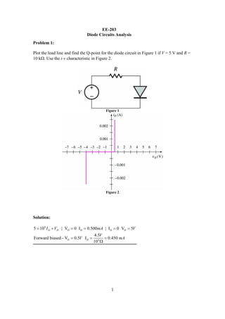
  • 1. EE-203 Diode Circuits Analysis Problem 1: Plot the load line and find the Q-point for the diode circuit in Figure 1 if V = 5 V and R = 10 kΩ. Use the i-v characteristic in Figure 2. Figure 1 Figure 2 Solution: 5 = 104 I D + VD | VD = 0 I D = 0.500mA | I D = 0 VD = 5V 4.5V Forward biased - VD = 0.5V ID = = 0.450 mA 104 Ω 1
  • 2. EE-203 Diode Circuits Analysis iD 2 mA 1 mA Q-point vD 1 2 3 4 5 Problem 2: Find the Q-point for the circuit in Figure 3 using the ideal diode model and constant voltage drop model with Von=0.6V. Figure 3 Solution : Ideal diode model: ID = 1V/10kΩ = 100 µA; (100 µA, 0 V) Constant voltage drop model: ID = (1-0.6)V/10kΩ = 40.0 µA; (40.0 µA, 0.6 V) 2
  • 3. EE-203 Diode Circuits Analysis Problem 3: Find the Q-point for the diode in Figure 4 using (a) the ideal diode model and (b) the constant voltage drop model with Von = 0.6 V. (c) Discuss the results. Which answer do you feel is most correct? Figure 4 Solution : Using Thévenin equivalent circuits yields and then combining the sources I I 1.2 k Ω 1k Ω 2.2 k Ω - V + - V + + + + 1.6 V 2V 0.4 V - - - (a) Ideal diode model: The 0.4 V source appears to be forward biasing the diode so we will assume it is "on". Substituting the ideal diode model for the forward region 0.4V yields I = = 0.182 mA . This current is greater than zero, which is consistent 2.2k Ω with the diode being "on". Thus the Q-pt is (0 V, +0.182 mA). 3
  • 4. EE-203 Diode Circuits Analysis I - V + 2.2 k Ω + 0.4 V - Ideal Diode: CVD: V on - + I 0.6 V 2.2 k Ω + 0.4 V - (b) CVD model: The 0.4 V source appears to be forward biasing the diode so we will assume it is "on". Substituting the CVD model with Von = 0.6 V yields 0.4V − 0.6V I= = −90.9 µ A . This current is negative which is not consistent with 2.2k Ω the assumption that the diode is "on". Thus the diode must be off. The resulting Q-pt is: (0.4 V, 0 mA). - V + I=0 2.2 k Ω + 0.4 V - (c) The second estimate is more realistic. 0.4 V is not sufficient to forward bias the diode into significant conduction. For example, let us assume that IS = 10-15 A and assume that the full 0.4 V appears across the diode. Then ⎡ ⎛ 0.4V ⎞ ⎤ iD = 10−15 A ⎢exp ⎜ − 1 = 8.89 nA , a very small current. ⎣ ⎝ 0.025V ⎟ ⎥ ⎠ ⎦ 4
  • 5. EE-203 Diode Circuits Analysis Problem 4: (a) Find I and V in the four circuits in Figure 5 using the ideal diode model. (b) Repeat using the constant voltage drop model with Von = 0.7 V. Figure 5 (a) 5 − ( −5) (a ) Diode is forward biased:V = − 5+0= − 5 V | I= = 0.500 mA 20k Ω (b) Diode is reverse biased: I =0 | V=7 − 20k Ω ( I ) = 7 V | VD = −10 V 3 − ( −7) (c) Diode is forward biased:V =3 − 0=3 V | I= = 0.500 mA 20k Ω (d ) Diode is reverse biased: I =0 | V= − 5 + 20k Ω ( I ) = −5 V | VD = −10 V (b) 5 − ( −4.3) (a ) Diode is forward biased:V = − 5+0.7= − 4.3 V | I= = 0.465 mA 20k Ω (b) Diode is reverse biased: I =0 | V=7 − 20k Ω ( I ) = 7 V | VD = −10 V 2.3 − ( −7) (c) Diode is forward biased:V =3 − 0.7=2.3 V | I= = 0.465 mA 20k Ω (d ) Diode is reverse biased: I =0 | V= − 5 + 20k Ω ( I ) = −5 V | VD = −10 V 5
  • 6. EE-203 Diode Circuits Analysis Problem 5: (a) Find I and V in the four circuits in Figure 5 using the ideal diode model if the resistor values are changed to 100 kΩ. (b) Repeat using the constant voltage drop model with Von = 0.6 V. Solution : (a) 5 − ( −5) (a ) Diode is forward biased:V = − 5+0= − 5 V | I= = 100 µ A 100k Ω (b) Diode is reverse biased: I =0 A | V=7 − 100k Ω ( I ) = 7 V | VD = −10 V 3 − ( −7 ) (c) Diode is forward biased:V =3 − 0=3 V | I= = 100 µ A 100k Ω (d ) Diode is reverse biased: I =0 A | V= − 5 + 100k Ω ( I ) = −5 V | VD = −10 V (b) 5 − ( −4.4) (a ) Diode is forward biased:V = − 5+0.6= − 4.4 V | I= = 94.0 µ A 100k Ω (b) Diode is reverse biased: I =0 | V=7 − 100k Ω ( I ) = 7 V | VD = −10 V 2.4 − ( −7) (c) Diode is forward biased:V =3 − 0.6=2.4 V | I= = 94.0 µ A 100k Ω (d ) Diode is reverse biased: I =0 | V= − 5 + 20k Ω ( I ) = −5 V | VD = −10 V 6
  • 7. EE-203 Diode Circuits Analysis Problem 6: Find the Q-points for the diodes in the circuits in Figure 6 using the ideal diode model. Figure 6 Solution : Diodes are labeled from left to right 10 − 0 (a ) D1 on, D 2 off, D3 on: ID2 = 0 | ID1 = = 1mA 3k Ω + 7 k Ω 0 − ( −5) I D3 + 1.00mA = → I D3 = 1.00mA | VD2 = 5 − (10 − 3000 I D1 ) = −2V 2.5k Ω D1:(1.00 mA, 0 V ) D 2 :( 0 mA, − 2 V ) D3:(1.00 mA, 0 V ) (b) D1 on, D 2 off, D3 off: I D2 = 0 | I D3 = 0 10 − ( −5) I D1 = = 0.500mA | VD2 = 5 − (10 − 8000 I D1 ) = −1.00V 8k Ω + 10k Ω + 12k Ω VD3 = − ( −5 + 12000 I D1 ) = −1.00V D1 : ( 0.500 mA, 0 V ) D2 : ( 0 A, − 1.00 V ) D3 : ( 0 A, − 1.00 V ) 7
  • 8. EE-203 Diode Circuits Analysis (c) D1 on, D 2 on, D3 on 0 − ( −10) 0 − ( 2) I D1 = = 1.25mA > 0 | I10K = = −0.200mA | I D 2 = I D1 + I10 K = 1.05mA > 0 8k Ω 10k Ω 2 − ( −5) I12K = = 0.583mA | I D 3 = I12 K − I10 K = 0.783mA > 0 12k Ω D1 : (1.25 mA, 0 V ) D2 : (1.05 mA, 0 V ) D3 : ( 0.783 mA, 0 V ) (d ) D1 off , D2 off , D3 on: I D1 = 0, I D 2 = 0 12 − ( −5) V I D3 = = 567µ A > 0 | VD1 = 0 − ( −5 + 10000 I D 3 ) = −0.667V < 0 30 kΩ VD2 = 5 − (12 − 10000 I D 3 ) = −1.33V < 0 D1 : ( 0 A, − 0.667 V ) D2 : ( 0 A, − 1.33 V ) D3 : ( 567 µ A, 0 V ) Problem 7: Find the Q-points for the diodes in the circuits in Figure 6 using the constant voltage drop model with Von = 0.6 V. Solution: Diodes are labeled from left to right 10 − 0.6 − ( −0.6) (a ) D1 on, D 2 off, D3 on: ID2 = 0 | ID1 = = 1.00mA 3k Ω + 7 k Ω −0.6 − ( −5) I D3 + 1.00mA = → I D3 = 0.760mA | VD2 = 5 − (10 − 0.6 − 3000 I D1 ) = −1.40V 2.5k Ω D1:(1.00 mA, 0.600 V ) D 2 :( 0 mA, − 1.40 V ) D3 :( 0.760 mA, 0.600V ) (b) D1 on, D 2 off, D3 off: I D2 = 0 | I D3 = 0 10 − 0.6 − ( −5) I D1 = = 0.480mA | VD2 = 5 − (10 − 0.6 − 8000 I D1 ) = −0.560V 8k Ω + 10k Ω + 12k Ω VD3 = − ( −5 + 12000 I D1 ) = −0.760V D1:( 0.480 mA, 0.600 V ) D 2 :( 0 A, − 0.560 V ) D3:( 0 A, − 0.760 V ) 8
  • 9. EE-203 Diode Circuits Analysis (c) D1 on, D 2 on, D3 on −0.6 − ( −9.4) V −0.6 − (1.4) V I D1 = = 1.10mA > 0 | I10 K = = −0.200mA 8 kΩ 10 kΩ 1.4 − ( −5) V I D 2 = I D1 + I10 K = 0.900mA > 0 | I12 K = = 0.533mA | I D 3 = I12 K − I10 K = 0.733mA > 0 12 kΩ D1:(1.10 mA, 0.600 V ) D 2 :( 0.900 mA, 0.600 V ) D3 :( 0.733 mA, 0.600 V) (d ) D1 off , D2 off , D3 on: I D1 = 0, I D 2 = 0 11.4 − ( −5) V I D3 = = 547 µ A > 0 | VD1 = 0 − ( −5 + 10000 I D 3 ) = −0.467V < 0 30 kΩ VD2 = 5 − (11.4 − 10000 I D 3 ) = −0.933V < 0 D1 : ( 0 A, − 0.467 V ) D2 : ( 0 A, − 0.933 V ) D3 : ( 547 µ A, 0 V ) 9