2. FIG. 2. Schematic cross section of the calibrated STM.
stage. With this stage, it is possible to scan in the X – Y plane
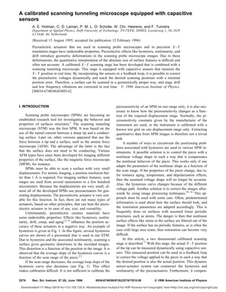
FIG. 1. Typical measured hysteresis curves of a piezostack as a result of
applying a triangular voltage shape to the piezo. Reducing the amplitude of
in a calibrated mode. The range is 10 m in X and Y direc-
the exciting voltage reduces the hysteresis but decreases the loop slope tions. The inchworm with tube scanner is mounted into the
piezosensitivity . center of the calibrated stage and is moved as a whole with
respect to the sample holder. The sample holder is placed on
sates in real time, drift, and low frequency vibrations in the a support plate.
X – Y scanning plane. The calibrated stage consists of a symmetrical set of
leafsprings made out of one piece of stainless steel Fig. 3 .
II. STM DESIGN The thickness of the leafsprings is 2 mm, their height is 20
mm, and their length is 15 mm. The hollow center cube of
A. Mechanical
the elastic system has a dimension of 20 20 20 mm and
The dynamic range of the STM is 10 m in X and Y the center hole has a diameter of 16 mm. The stiffness of the
directions and 1.5 m in the Z direction. The STM is opti- elastic system in X and Y directions is 8 107 N m 1. The
mized for operating in the scanning range of 100 nm to 10 leafspring system is connected to the ‘‘fixed world’’ at the
m. In these ranges, the hysteresis and nonlinearity cannot corner points of the leafspring system. On the side blocks, a
be neglected. The environments in which the STM must op- force is applied in the X and Y directions by means of the X
erate are air and ultrahigh vacuum UHV . and Y piezostack (F x ,F y ). These stacks are mounted outside
The basic considerations that are related to an STM de- the system. The piezostacks19 have a length of 20 mm. With-
sign in general are symmetry and stiffness. Building a sym- out a preload force, they are able to extend 20 m.3 At the
metrical design is favorable for the thermal properties of the opposite side of the piezostacks, a preload force is applied to
stage. A symmetrical setup will also result in an equal me- the leafspring system through spiral springs (F sx ,F sy ).
chanical behavior in X and Y directions. The coupling be- These springs increase the stiffness and symmetry of the sys-
tween X and Y must be minimal. Our design presents an tem. It is also possible to use elastic elements
elegant solution to these specifications, as will be shown
later on. Increasing the stiffness in X and Y directions is
necessary for reducing the vibration sensitivity in X and Y . A
larger stiffness results in a higher resonance frequency, al-
lowing higher scanning speeds and a better dynamic re-
sponse. A stiffer design can be achieved by increasing the
thickness of elastic elements or by an overall reduction of the
size of the elastic elements. If a design is stiffer, then the
forces the piezos must deliver for a given displacement are
higher. This results in a reduced expansion range of the
piezo.3 In this, a tradeoff must be found. A compromise must
be made between the desire to reduce the overall size and
mass for increased stiffness and the size necessary to incor-
porate the capacitive sensors. In our prototype, the accent is
placed on the size of the capacitive sensors.
In the STM, two scanning mechanisms are incorporated.
First, the STM has a traditional scanning stage. This stage is
a commercial ARIS 11 STM.18 It contains an inchworm with
a tube scanner on top of it see Fig. 2 . The inchworm is used
for coarse positioning of the STM tip in the Z direction. The
tube scanner allows fast scanning and atomic imaging. Scan-
FIG. 3. Schematic topview of the leafspring system of the scanning stage.
ning with the tube gives all the problems related to the use of
Capacitive sensors are mounted at the locations X1, X2, Y 1, and Y 2 and
piezos. This tube scanner has an X – Y range of about 5 m measure the displacement of the hollow center cube. Forces are applied at
and a Z range of 1.5 m. The second stage is the calibrated the locations indicated with arrows.
Rev. Sci. Instrum., Vol. 67, No. 6, June 1996 Calibrated STM 2275
Downloaded¬11¬May¬2010¬to¬131.155.135.0.¬Redistribution¬subject¬to¬AIP¬license¬or¬copyright;¬see¬http://rsi.aip.org/rsi/copyright.jsp
3. with flexural hinges instead of leafsprings. The only draw-
back is that the mass of the moving parts of the construction
will increase, resulting in a lower resonance frequency.
The special character of this elastic system is the sym-
metry as a whole. Both the X and Y actuators are connected
to the ‘‘fixed world.’’ The stiffness in the Z direction is quite
high because the leafsprings are very stiff in this direction.
Looking at the elastic X and Y behavior, one can say that
from the X piezo point of view, the Y direction is very stiff
because the leafsprings in the Y direction are loaded in their
stiffest direction. Also, from the Y piezo point of view, the X
direction is very stiff for the same reasons. A small X – Y
coupling exists due to the fact that bending the leafsprings in,
for instance, the X direction will generate a force that tries to
bend the leafsprings in the Y direction. If the system operates
in a dynamic feedback mode using sensors, as will be dis-
cussed later, then this coupling will not present any problem.
FIG. 4. a Detail of the location of the sensor electrodes for one direction.
B. Capacitive sensors Two capacitors are used for measuring the translation of the center cube
with respect to the support plate on which the sample holder is placed. b
To calibrate small piezo movements, several sensing op- The shape of the electrode patterns of the two electrode plates of one ca-
tions are available. Optical sensing20 is widely used because pacitor is shown. Pattern type I consists of four subelectrodes to measure
of its success in AFM microscopes. X-ray calibration21 is plate tilting. To measure displacement, the four subelectrodes are connected
together to form one capacitor. The measuring electrodes are surrounded by
proposed also but this is only usable in a controlled labora- guarding electrodes.
tory situation. We have opted for capacitive sensors. These
types of sensors are simple, predictable, and usable in a wide
range of environments. Several authors have incorporated Using special design rules,25 the capacitor fringing ef-
capacitive sensors into a STM.22–24 For proper use of these fects are virtually eliminated in the electrode design. The
sensors, a good knowledge and experience in the design and reason is that three terminal capacitor geometries are used
measurement of capacitive sensors is needed.25 The way in that use guarding electrodes around the capacitor electrodes.
which capacitive sensors are combined with a mechanical This makes the capacitance versus distance relation very pre-
system is very important. A mechatronic approach is often dictable. The only practical problem is that the electrode
necessary. plates are always tilted with respect to each other. This tilt is
To measure the X – Y displacement of the STM tip accu- second order in the tilting angles. For that reason, some elec-
rately, the sensors are placed as close as possible around the trodes are divided into four subelectrodes, see Fig. 4 b , type
center. Any distance between the point of interest center, I. By measuring the capacitance of the subelectrodes and
tip and the sensor introduces a position uncertainty due to combining the results, it is possible to measure the tilt of the
the behavior of the ‘‘material path’’ between the sensor and capacitor plates in two directions. In reality, the tilting of the
the center. This uncertainty is almost inevitable from a con- electrodes is small and fixed. It is therefore almost never
structional point of view. The effect can be minimized by necessary to compensate for tilting effects, but if required,
reducing this distance and by making the construction sym- they can be incorporated into the capacitance relation.
metrical. For that reason, the electrode plates of the capaci- The plate distances used for the capacitors have an av-
tors are mounted at the sides of the center cube. Four pairs of erage value of 220 m, resulting in a nominal capacitance of
electrode plates are used. The counter electrode plates are 3.2 pF. The capacitance detectors are based on a transformer
mounted on the support plate with the sample holder. This ratio bridge with a low impedance current-to-voltage pre-
support plate is used as a reference plate. In Fig. 4 a , this amplifier and a synchronous detector operating on a fre-
construction is illustrated for one translation direction. quency of 62.5 kHz for the X direction and 46.9 kHz for the
As is seen in this figure, two sets of capacitor plates are Y direction. With this detector system, it is possible to mea-
being used for measuring one direction. If the center cube is sure attofarrads with a bandwidth of more than 1 kHz and
translated over a distance x, then the plate distance of capaci- with a stability of 10 ppm. The accuracy, noise, and stability
tor X 1 is increased by x, reducing the capacitance C 1 . The of the capacitance detectors determine the achievable abso-
plate distance of capacitor X 2 is decreased by x, increasing lute position accuracy, the detectors are therefore calibrated
the capacitance C 2 . Subtracting C 2 from C 1 using a trans- using standard reference capacitors. Subnanometer position
former ratio bridge circuit2 gives a capacitance change that is resolution is possible with these detectors,2 although the sys-
strongly related to the change x and can be described exactly tem is optimized for larger scan ranges. The position resolu-
with a capacitance expression in which geometric and plate tion of the calibrated stage presented here is better than 2 nm
tilting information is used. Taking a large distance for the over the full scan range of 10 m.
capacitors compared to the scanning displacements, the ca- The capacitor plates are made of quartz mask plates. The
pacitance to displacement relation can be considered linear. electrodes are fabricated using a electron beam pattern gen-
2276 Rev. Sci. Instrum., Vol. 67, No. 6, June 1996 Calibrated STM
Downloaded¬11¬May¬2010¬to¬131.155.135.0.¬Redistribution¬subject¬to¬AIP¬license¬or¬copyright;¬see¬http://rsi.aip.org/rsi/copyright.jsp
4. FIG. 6. Upper graph: the measured hysteresis shift between the LR and RL
image of Fig. 5 where a tube scanner is used for scanning. Bottom graph:
FIG. 5. Composition of four images taken with the tube scanner of the same the measured hysteresis shift between the TB and BT image of Fig. 5 where
area of a reference surface and with different scanning directions. In the a tube scanner is used for scanning.
top-left image the scanning direction is left to right LR . In the bottom-left
image the scanning direction is RL. In the top-right image the scanning
direction is top to bottom TB . The bottom-right image is scanned BT.
necessary for following the surface. In this situation, the lat-
Equal features in the images are indicated with markers in the images. The eral scanning movements are calibrated also.
reference surface has features with a square period of 707 nm.
III. RESULTS
erator EBPG with a writing accuracy better than 100 nm To test the performance of the developed STM, a plati-
and are covered with gold electrodes. num coated reference grid is used with a square period of
The differential geometry that uses two sets of capacitor 707 nm.26 With this reference grid, it is possible to compare
plates has a clear advantage compared to a single plate mea- the imaging properties of the tube scanner, the calibrated
surement. The linearity and sensitivity is better and the sen- stage without calibration, and the calibrated stage in cali-
sitivity for thermal expansion of the stage as a whole is re- brated feedback mode. To judge the STM images, it is not
duced. The capacitance offset that is always present with sufficient to record one image of the surface. To get infor-
only one capacitor is removed by subtracting the offset of the mation about hysteresis, it is necessary to acquire four im-
other capacitor. This allows us to amplify the displacement ages of the same surface and close in time after each other.
information in the detector much more than compared to the These images must differ in the scanning direction used. The
single plate capacitor situation. From a measurement point of first image is scanned with the scan line going from left to
view, it would be very disadvantageous to look at capaci- right LR and starting in the top-left corner. The second is
tance changes in the attofarrad range on top of a dc signal of the retrace scan line RL . In the third image, the scanning
3 pF. direction is rotated 90°, resulting in a scanline going from the
With the dual stage design, it is possible to scan in sev- top of the image to the bottom TB and starting in the top-
eral different ways. The calibrated stage can be used for right corner. The fourth image is the retrace scanline BT .
generating a calibrated X – Y , offset while the tube scanner Some of the images contain double tip effects. These tip
scans the surface in a normal fashion. This scanning mode artifacts presented no problem in judging the hysteresis ef-
allows small area tube scanning say, for instance, 30 30 fects.
nm with long range position accuracy.
A. Tube scanner
The other scan mode is scanning solely with the cali-
brated stage. The sensor information is used in a feedback In Fig. 5 the result of a scan of the reference surface with
loop to correct the piezovoltages to achieve the correct X – Y the tube scanner and with a scan range of 8.3 m 8.3 m
position. In this mode, the tube segments are connected to- is shown. These images of 512 512 pixels are taken with a
gether and used exclusively for performing the Z motion scan speed of 500 ms/line. The displayed images are plane
FIG. 7. This sequence of STM images of a reference surface show the geometric distortions and drift caused by creep. The reference surface has features with
a square period of 707 nm.
Rev. Sci. Instrum., Vol. 67, No. 6, June 1996 Calibrated STM 2277
Downloaded¬11¬May¬2010¬to¬131.155.135.0.¬Redistribution¬subject¬to¬AIP¬license¬or¬copyright;¬see¬http://rsi.aip.org/rsi/copyright.jsp
5. FIG. 10. The measured hysteresis shifts of Figs. 8 and 9 are shown here,
where the piezostack of the system is used for scanning. The measured shifts
of Fig. 8 are indicated with filled circles . The measured shifts of Fig. 9
are indicated with filled squares . The scanning area of Fig. 9 two times
smaller than the scanned area of Fig. 8.
the images to indicate a similar surface feature in the images.
If there is no hysteresis present, then the four images must be
geometrically identical. It is obvious that this is not the case.
Comparing the LR and RL images, similar features in the
two images have different sizes and are shifted in the X
direction due to hysteresis of the tube scanner. Comparing
the Y direction in the LR and RL images, no shift is observ-
able, but the Y location of the features is not correct due to
the nonlinearity of the Y scan. Comparing the TB and BT
FIG. 8. Scanning an area of the reference surface with the calibrated stage
scans, the situation is reversed. Similar surface features are
gives these images. The scan range is 6.4 m 6.4 m. The top image is
scanned LR and the bottom image is scanned RL. In this recording, the Y shifted in the Y direction due to the hysteresis in the Y di-
direction is calibrated and the X diretion is not. The reference surface has rection.
features with a square period of 707 nm. The shift in the images is analyzed using image process-
ing techniques to extract similar surface features and to de-
subtracted and contrast stretched to exemplify the hysteresis termine their average x,y pixel location in each of the four
properties. For the same reason, the RL image is placed be- images. In the upper part of Fig. 6 this is done for the LR-RL
low the LR image. The hysteresis shift is then more appar- images. In this figure, the measured shift of a surface feature
ent. For reference clarity, round markers are placed inside is plotted against the X position of the feature in the LR
image. In the lower graph of Fig. 6 this is also done for the
Y shift in the TB and BT images.
The X and Y shifts between two images have a distinct
parabolic shape. The maximum shift between two similar
features on the surface is 74 pixels for the LR-RL image.
From the reference grid, it is found that the total scan range
is 8.3 m 8.3 m. The shift in an image is therefore
equivalent with some 1.2 m. This is almost 15% of the total
scan range. For the maximum Y shift, we find 76 pixels. This
would mean that the X and Y directions of the tube scanner
have different piezoconstants. This difference is some 2% to
3%, although this small deviation could be explained also
with the inaccuracies of the analysis method. In Fig. 6 it is
seen that the maximum shift in the images is not located in
the middle of the images but is shifted towards the side of
the image. Extrapolating the graphs to the x pixel coordi-
nates 0 and 511, it is found that the shift is practically zero at
these coordinates. This is to be expected, because the scan-
ning direction of the piezovoltage is reversed here.
An other piezoelectric effect is creep. This is a delayed
response of the piezo on piezoelectric voltage changes. This
effect should not be underestimated. In Fig. 7 a sequence of
images is displayed that shows how creep can influence the
geometric appearance of STM images in time and in a worst
case situation. These images were recorded as follows.
FIG. 9. Scanning the same area with half the scan range 3.2 m 3.2 m
of the previous image and under the same conditions results in these two First, the offset voltages on the tube segments were
images. taken as V Xoff 80 V, V Y off 80 V. After a stabilization
2278 Rev. Sci. Instrum., Vol. 67, No. 6, June 1996 Calibrated STM
Downloaded¬11¬May¬2010¬to¬131.155.135.0.¬Redistribution¬subject¬to¬AIP¬license¬or¬copyright;¬see¬http://rsi.aip.org/rsi/copyright.jsp
6. direction and switched off for the X direction. This means
that the image is geometrically correct in the Y direction and
still suffers from hysteresis for the X direction. In Fig. 8, a
scan is made of the surface using a scan range of 6.4 m.
The size of the image is 256 256 pixels and the scan speed
is 3 s/line. In Fig. 9, a smaller area of 3.2 m is scanned.
Only LR and RL images are used. Analyzing the shift in the
X direction for the two scan ranges, a graph is obtained as
shown in Fig. 10. The measured shifts exhibit a parabolic
shape similar to the shifts of the tube scanner. The maximum
shift is different compared to the tube situation because the
scan ranges are not the same and the piezoconstant of the
tube and the stacks are different. The shift of the reduced
scan area is smaller, as is expected from the smaller scan
area. Although the scanned area of Fig. 9 is twice as small as
the scan of Fig. 8, the shift is not twice as small as the shift
of the larger scan area. This indicates a nonlinear scaling
behavior. What is visible in the shift graphs of the pi-
ezostacks is that the maximum of the shift is not located in
the middle of the image. This same feature was observed
with the tube scanner.
If both the feedback of the X and Y direction is used, a
fully calibrated scan is obtained. In Fig. 11, this LR and RL
FIG. 11. Scanning a large area of the reference surface in calibrated feed- image is shown. These images have a size of 512 512 pix-
back mode for X and Y gives these two images of the reference surface. The els and are scanned with a speed of 1 s/line and with a scan
top image is scanned LR and the bottom image is scanned RL. The refer- range of 8.6 m. The geometric distortion is minimal. The
ence grid has a period of 500 nm.
reference grid is square and straight as desired. For these
images, the shift analysis has been performed as before. In
time of 15 min, the offset voltages were changed manually to Fig. 12 the result is shown. The measured shifts of similar
V Xoff 80 V, V Y off 80 V as fast as possible. objects in the LR and RL image appear quite random, al-
Directly after this voltage step, seven images of 128 128 though it looks like there is a bias shift of some 3 pixels
pixels 30 V 30 V scan width were taken rapidly after present. This is presumably caused by a dynamic feedback
each other with the tube scanner. Every image took some 26 error. The apparent randomness is probably caused by the
s to complete 200 ms/line . From the images, it is clear that inaccuracies of the image processing analysis and by the dif-
the first image taken is extremely distorted. The following ference in image quality of the LR and RL image. Convert-
images show the slow relaxation of the tube scanner. But ing the output of the capacitive sensor system into displace-
even after the last image 182 s , the relaxation drift contin- ments is done by the capacitance-to-displacement relation,
ued. Only a feedback controlled calibrated STM could coun- which is known accurately and translates picofarads into na-
teract this creep effect. nometers.
B. The calibrated stage
ACKNOWLEDGMENT
Imaging the reference grid with the calibrated stage can
be done in two ways. First, it is possible to scan with the The authors wish to thank H. Vogelaar for his contribu-
piezostacks, ignoring the sensor information. Second, it is tions in the fabrication of the calibrated STM.
possible to switch on the sensor system and scan the surface
in a calibrated fashion using the sensors in feedback mode. 1
J. Jahanmir, B. G. Haggar, and J. B. Hayes, Scanning Microsc. 6, 625
In Figs. 8 and 9, a combination of the scan types is used. 1992 .
In these STM images, the feedback is switched on for the Y 2
A. E. Holman, W. Chr. Heerens, and F. Tuinstra, Sensors Actuators A 36,
37 1993 .
3
A. E. Holman, P. M. L. O. Scholte, W. Chr. Heerens, and F. Tuinstra,
Rev. Sci. Instrum. 66, 3208 1995 .
4
L. Libioulle, A. Ronda, M. Taborelli, and J. M. Gilles, J. Vac. Sci. Tech-
nol. B 9, 655 1991 .
5
L. E. C. van de Leemput, P. H. H. Rongen, B. H. Timmerman, and H. van
Kempen, Rev. Sci. Instrum. 62, 989 1991 .
6
K. G. Vandervoort, R. K. Zasadzinski, G. G. Galicia, and G. W. Crabtree,
Rev. Sci. Instrum. 64, 896 1993 .
7
S. Vieira, IBM J. Res. Devel. 30, 553 1986 .
8
R. W. Basedow and T. D. Cocks, J. Phys. E 13, 840 1980 .
9
S. M. Hues, C. F. Draper, K. P. Lee, and R. J. Colton, Rev. Sci. Instrum.
FIG. 12. Measuring the hysteresis shift of the LR and RL image in the 65, 1561 1994 .
10
calibrated feedback mode of Fig. 11 results in this shift graph. J. E. Griffith and D. A. Grigg, J. Appl. Phys. 74, R83 1993 .
Rev. Sci. Instrum., Vol. 67, No. 6, June 1996 Calibrated STM 2279
Downloaded¬11¬May¬2010¬to¬131.155.135.0.¬Redistribution¬subject¬to¬AIP¬license¬or¬copyright;¬see¬http://rsi.aip.org/rsi/copyright.jsp
7. 11
”
J. F. Jorgensen, L. L. Madsen, J. Garnaes, K. Carneiro, and K. Schaum- 20
R. C. Barrett and C. F. Quate, Rev. Sci. Instrum. 62, 1393 1991 .
burg, J. Vac. Sci Technol. B 12, 1698 1994 . 21
D. K. Bowen, D. G. Chetwynd, and D. R. Schwarzenberger, Meas. Sci.
12
”
J. F. Jorgensen, K. Carneiro, L. L. Madsen, and K. Conradsen, J. Vac. Sci Technol. 1, 107 1990 .
Technol. B 12, 1702 1994 . 22
J. E. Griffith, G. L. Miller, C. A. Green, D. A. Grigg, and P. E. Russell, J.
13
”
J. F. Jorgensen, K. Carneiro, and L. L. Madsen, Nanotechnol. 4, 152 Vac. Sci. Technol. B 8, 2023 1990 .
1993 . 23 ˇ `
14 S. Desogus, S. Lanyi, R. Nerino, and G. B. Picotto, J. Vac. Sci. Technol.
S. Carrara, P. Facci, and C. Nicolini, Rev. Sci. Instrum. 65, 2860 1994 .
15 B 12, 1665 1994 .
E. P. Stoll, Rev. Sci. Instrum. 65, 2864 1994 . 24
16
V. Yu. Yurov and A. N. Klimov, Rev. Sci. Instrum. 65, 1551 1994 . O. Jusko, X. Zhao, H. Wolff, and G. Wilkening, Rev. Sci. Instrum. 65,
17
Patent pending. 2514 1994 .
25
18
Burleigh Instruments, Inc., Burleigh Park, Fishers, NY 14453. W. Chr. Heerens, J. Phys. E 19, 897 1986 .
19 26
PI Physik Instrumente GmbH & Co., Waldbronn, Germany. Type P178.20 Fabricated at the Philips Research Laboratory, Eindhoven, the Nether-
with UHV option. lands.
2280 Rev. Sci. Instrum., Vol. 67, No. 6, June 1996 Calibrated STM
Downloaded¬11¬May¬2010¬to¬131.155.135.0.¬Redistribution¬subject¬to¬AIP¬license¬or¬copyright;¬see¬http://rsi.aip.org/rsi/copyright.jsp