
Recomendados
Mais conteúdo relacionado
Mais procurados
Mais procurados (20)
Destaque
Destaque (20)
Semelhante a Precise Hall-Effect ICs for Automotive and Industrial Applications
Semelhante a Precise Hall-Effect ICs for Automotive and Industrial Applications (20)
Último
Último (20)
Precise Hall-Effect ICs for Automotive and Industrial Applications
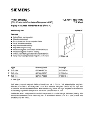
- 1. Ψ-Hall-Effect IC; TLE 4904; TLE 4934; (PSI: Protected-Precision-Siemens-Hall-IC) TLE 4944 Highly Accurate, Protected Hall-Effect IC Preliminary Data Bipolar-IC Features q Active Piezo compensation q Digital output signal q For unipolar and bipolar magnetic fields q Large temperature range q High temperature stability q High switching accuracy q Protection against overvoltage and short circuit q Protection against reversed polarity q Output protection against electrical disturbances q Temperature compensated magnetic perfomance P-SSO- 3-4 Type Ordering Code Package w TLE 4904 Q67006-A9011 P-SSO-3-4 w TLE 4934 Q67006-A9027 P-SSO-3-4 w TLE 4944 Q67006-A9028 P-SSO-3-4 w New type TLE 4904 (Unipolar Magnetic Fields - Switch) and the TLE 4934, TLE 4944 (Bipolar Magnetic Fields-Latch/Switch) are integrated circuit Hall sensors designed specifically for high end automotive and industrial electronics. Precise switching points and high temperature stability are achieved by adjustment temperature and active compensation on chip. These Hall effect integrated circuits include protection for overvoltage, reversed polarity and electrical overstress such as load dump, etc., in accordance with ISO-TR 7637 (DIN 40 839) and short circuit of the output.
- 2. TLE 4904; TLE 4934; TLE 4944 Pin Configuration (top view) Pin Definition and Functions Pin Symbol Function VS 1 Supply voltage 2 GND Ground 3 Q Output
- 3. TLE 4904; TLE 4934; TLE 4944 Circuit Description The circuit includes Hall generator, amplifier and comperator with hysteresis on one chip. The internal reference provides the supply voltage for the components. A magnetic field perpendicular to the chip surface induces a voltage at the hall probe. This voltage is amplified and switches a comparator with open-drain output. The switching points are adjusted to achieve high accuracy. The active offset compensation eliminates internal and external offsets (mechanical stress) by switching of the hall element. The built-in temperature compensation fits to regular magnet system. Protection is provided at the input/supply (pin 1) for overvoltage and reverse polarity, against overstress such as load dump, etc., in accordance with ISO-TR 7637 (DIN 40839). The output (pin 3) is protected against voltage peaks and short circuit. Figure 1 Block Diagram
- 4. TLE 4904; TLE 4934; TLE 4944 Functional Description When a positive magnetic field is applied in the indicated direction (figure 2) and the turn-ON magnetic induction BOP is exceeded, the output of the Hall-effect IC will conduct (Operate Point). When the current is reduced (TLE 4904) or a reverse magnetic field is generated (TLE 4934, TLE 4944), the output of the IC turns OFF (Release Point) (figures 3 and 4). BRP and BOP are the critical parameters in most unipolar and bipolar Hall-switch applications. For this reason the switching points are adjusted. Figure 2 Sensor/Magnetic-Field Configuration
- 5. TLE 4904; TLE 4934; TLE 4944 Figure 3 Switching Characteristics TLE 4904 Figure 4 Switching Characteristics TLE 4934, TLE 4944
- 6. TLE 4904; TLE 4934; TLE 4944 Absolute Maximum Ratings TA = – 40 to 125 ˚C Parameter Symbol Limit Values Unit Remarks min. max. VDD Supply voltage – 40 28 V – VQ Output voltage – 28 V – IQ Output short circuit current – 150 mA – °C Tj OFF Output thermal protection 170 200 – °C Tj ON 135 165 °C Tj Junction temperature – 40 150 – °C Tj Junction temperature – 170 1000 h °C Tj Junction temperature – 210 40 h °C Tstg Storage temperature – 40 150 – Rth JA Thermal resistance – 190 K/W – IDDZ t < 2 ms; v = 0.1 Current through input- – 200 200 mA protection device IQZ t < 2 ms; v = 0.1 Current through output- – 200 200 mA protection device Operating Range VS Supply voltage 3.8 24 V – °C Tj Junction temperature – 40 150 – °C Tj Junction temperature – 40 170 threshold may exceed the limits
- 7. TLE 4904; TLE 4934; TLE 4944 AC/DC Characteristics 4.5 V ≤ VDD ≤ 24 V; – 40 ˚C ≤ Tj ≤ 150 ˚C Parameter Symbol Limit Values Unit Test Condition Test Circuit min. typ. max. IS B < BRP Supply current – 1.5 3 mA 1 IS B > BOP – 1.5 3 mA 1 Output saturation voltage VQSat IQ = 40 mA – 0.25 0.6 V 2 µA IQL VQ = 24 V Output leakage current – – 10 2 Overvoltage protection IS = 10 mA, 25 °C 2 VSZ –at supply voltage 28 31 – V IQ = 10 mA, 25 °C 2 VQZ –at output 28 31 – V µs tdHL / tdLH – Delay time 50 75 – 1 Magnetic Characteristics 3.8 V ≤ VDD ≤ 24 V Parameter Symbol Limit Values Unit -40 ˚C 25 ˚C 150 ˚C min. typ. max. min. typ. max. min. typ. max. TLE 4904 TC = – 0.04 %/˚C BOP 9.2 10.8 12.3 9 10.5 12 8.5 10 11.4 mT BRP 5.1 6.2 7.2 5 6 7 4.7 5.7 6.7 mT BHy 4.1 4.6 5.1 4 4.5 5 3.8 4.3 4.8 mT TLE 4934 TC = – 0.2 %/˚C BOP 11.9 11.9 13.6 9 10.5 12 6.7 7.9 9 mT BRP -13.6 -11.9 -10.2 -12 -10.5 -9 -9 -7.9 -6.7 mT BHy 21.4 23.8 26.2 19 21 23 14.2 15.8 17.4 mT TLE 4944 TC = – 0.2 %/˚C BOP 3.9 5.1 6.2 3.5 4.5 5.5 2.6 3.4 4.1 mT BRP -6.2 -5.1 -3.9 -5.5 -4.5 -3.5 -4.1 -3.4 -2.6 mT BHy 9.2 10.2 11.2 8 9 10 6.1 6.8 7.5 mT
- 8. TLE 4904; TLE 4934; TLE 4944 Figure 5 Test Circuit 1 Figure 6 Test Circuit 2
- 9. TLE 4904; TLE 4934; TLE 4944 Figure 7 Diagram Figure 8 Application Circuit