SlideShare uma empresa Scribd logo
1 de 5
Topic: Integrated Circuit Fabrication
Researched By: Johnmar T. Diamante ECE5A
What is an Integrated Circuit?
An integrated circuit (IC), sometimes called a chip or microchip, is a semiconductor wafer on which
thousands or millions of tiny resistors, capacitors, and transistors are fabricated. An IC can function as an
amplifier, oscillator, timer, counter, computer memory, or microprocessor. A particular IC is categorized
as either linear (analog) or digital, depending on its intended application.
Linear ICs have continuously variable output (theoretically capable of attaining an infinite number of
states) that depends on the input signal level. As the term implies, the output signal level is a linear
function of the input signal level. Ideally, when the instantaneous output is graphed against the
instantaneous input, the plot appears as a straight line. Linear ICs are used as audio-frequency (AF) and
radio-frequency (RF) amplifiers.
Digital ICs operate at only a few defined levels or states, rather than over a continuous range of signal
amplitudes. These devices are used in computers, computer networks, modems, and frequency
counters. The fundamental building blocks of digital ICs are logic gates, which work with binary data,
that is, signals that have only two different states, called low (logic 0) and high (logic 1).
Processes in IC Fabrication:
Silicon Wafer Fabrication:
1. Converting sand to silicon
Sand is composed of silica and is the starting point for making a silicon wafer. To extract the
element silicon from the silica, it must be reduced. This is accomplished by heating a mixture of
silica and carbon in an electric arc furnace to a temperature in excess of 2,000°C. Impurities such as
iron, aluminum, boron and phosphorous also react to give their chlorides, which are then removed
by fractional distillation. During the reaction, silicon is deposited on the surface of an electrically
heated ultra-pure silicon rod to produce a silicon ingot.
2. Creating a cylindrical crystal
To turn it into a usable material, the silicon must be turned into single crystals that have a regular
atomic structure. This transformation is achieved through the Czochralski Process. Electronic-grade
silicon is melted in a rotating quartz crucible and held at just above its melting point of 1,414°C.
3. Slicing the crystal into wafers
Integrated circuits are approximately linear, which is to say that they're formed on the surface of the
silicon. To maximize the surface area of silicon available for making chips, the silicon ingot is sliced
up into discs called wafers. The wafers are just thick enough to allow them to be handled safely
during semiconductor fabrication. 300mm wafers are typically 0.775mm thick. Sawing is carried out
using a wire saw that cuts multiple slices simultaneously, in the same way that some kitchen gadgets
cut an egg into several slices in a single operation.
4. Making a patterned oxide layer
The wafer is heated to a high temperature in a furnace. The wafer is spun in a vacuum so that the
photoresist spreads out evenly over the surface before being baked dry. The wafer is exposed to
ultraviolet light through a photographic mask or film. The next stage is to develop the latent circuit
image. The photoresist isn't sufficiently durable to withstand the hot gasses used in some steps, but
it is able to withstand hydrofluoric acid, which is now used to dissolve those parts of the silicon
oxide layer where the photoresist has been washed away. Finally, a solvent is used to remove the
remaining photoresist, leaving a patterned oxide layer in the shape of the required circuit features.
Wafer Testing:
Wafer testing is a step performed during semiconductor device
fabrication. During this step, performed before a wafer is sent to die
preparation, all individual integrated circuits that are present on the
wafer are tested for functional defects by applying special test
patterns to them. The wafer testing is performed by a piece of test
equipment called a wafer prober.
Wafer Mounting:
To facilitate the processing of the wafer at wafer saw, support is
provided to the wafer by mounting the wafer on dicing tape. The
dicing tape is a PVC sheet typically 3 mm in thickness with synthetic
adhesive on one side to hold both the wafer frame and the wafer.
Dicing or Wafer Sawing:
Wafer saw follows wafer mounting and is the step that actually cuts
the wafer into individual dice for assembly in IC packages. The wafer
saw process consists of the following steps:
1. The frame-mounted wafer is automatically aligned into
position for cutting;
2. The wafer is then cut thru its thickness according to the programmed die dimensions using a
resin-bonded diamond wheel rotating at a very high rpm;
3. The wafer goes through a cleaning process using high pressure DI water sprayed on the
rotating wafer and then dried by air-blowing.
Die Bonding or Die Attach:
Die Bonding is the process of attaching the silicon chip to
the die pad or die cavity of the support structure of the
semiconductor package. These are the two common die
attach processes:
1. Adhesive Die Attach - uses adhesives such as polyimide, epoxy and silver-filled glass as die
attach material to mount the die on the die pad or cavity. The adhesive is first dispensed in
controlled amounts on the die pad or cavity. The die for mounting is then ejected from the
wafer by one or more ejector needles. While being ejected, a pick-and-place tool commonly
known as a 'collet' then retrieves the die from the wafer tape and positions it on the
adhesive.
2. Eutectic Die Attach - is commonly employed in hermetic packages, uses a eutectic alloy to
attach the die to the cavity. A eutectic alloy is an alloy with the lowest melting point possible
for the metals combined in the alloy. The Au-Si eutectic alloy is the most commonly used die
attach alloy in semiconductor packaging.
Wire Bonding:
Wire bonding is the process of providing electrical connection between
the silicon chip and the external leads of the semiconductor device using
very fine bonding wires. The wire used in wire bonding is usually made
either of gold (Au) or aluminum (Al), although Cu wire bonding is starting
to gain a foothold in the semiconductor manufacturing industry. These
are the two common wire bonding processes:
1. Gold ball wire bonding - a gold ball is first formed by melting the end of the wire through
electronic flame-off (EFO). The free-air ball is then brought into contact with the bond pad.
Adequate amounts of pressure, heat, and ultrasonic forces are then applied to the ball for a
specific amount of time, forming the initial metallurgical weld between the ball and the
bond pad as well as deforming the ball bond itself into its final shape. The wire is then run to
the corresponding finger of the lead frame, forming a gradual arc or "loop" between the
bond pad and the lead finger. Pressure and ultrasonic forces are applied to the wire to form
the second bond, this time with the lead finger.
2. Aluminum wedge wire bonding - a clamped aluminum wire is brought in contact with the
aluminum bond pad. Ultrasonic energy is then applied to the wire for a specific duration
while being held down by a specific amount of force, forming the first wedge bond between
the wire and the bond pad. The wire is then run to the corresponding lead finger, against
which it is again pressed. The second bond is again formed by applying ultrasonic energy to
the wire. The wire is then broken off by clamping and movement of the wire.
Molding or IC encapsulation:
Molding is the process of encapsulating the device in plastic material.
Transfer molding is one of the most widely used molding processes in
the semiconductor industry because of its capability to mold small
parts with complex features. In this process, the molding compound is
first preheated prior to its loading into the molding chamber.
After pre-heating, the molding compound is forced by a hydraulic plunger into the pot where it reaches
melting temperature and becomes fluid. The plunger then continues to force the fluid molding
compound into the runners of the mold chase. These runners serve as canals where the fluid molding
compound travels until it reaches the cavities, which contain the lead frames for encapsulation.
Plating or Lead Finish:
Plating or Lead Finish is the process of applying a coat of metal over the leads of an IC to protect the
leads against corrosion, protect the leads against abrasion, improve the solderability of the leads and
improve the appearance of the leads. These are the two widely used lead finish techniques in the
semiconductor industry:
1. Tin plating - is a form of pure metal electroplating, which is the process of depositing a
coating of metal on a surface by passing a current through a conductive medium, or
electrolyte.
2. Solder plating - is a form of alloy plating. An alloy is composed of at least two elements, at
least one of which is a metal. An alloy has better properties than its component metals: it is
harder, more corrosion-resistant, has better solderability and better appearance.
Marking:
Marking is the process of putting identification, traceability, and distinguishing
marks on the package of an IC. The device name, company logo, date code,
and lot id are examples of information commonly marked on the IC's package.
Some marks are put on the package during Assembly and some marks are put
on the package during Test. These are the two common marking processes:
1. Laser marking - as the name implies, refers to the process of engraving marks on the
marking surface using a laser beam. There are many types of lasers, but the ones used or in
use in the semiconductor industry include the CO2 laser, the YAG laser, and diode lasers.
2. Ink marking - consists of transferring an ink pattern from the plate, which is a flat block with
pattern depressions that are filled with ink, to the package, using a silicone rubber stamp
pad. Silicone rubber repels ink, making the transfer of the ink pattern clean and efficient. It
is also resilient and elastic, making it possible to print even on uneven surfaces.
Deflash/ Trim & Form /IC Singulation:
Deflash - removal of flashes from the package of the newly molded parts.. Flashes are the excess plastic
material sticking out of the package edges right after molding.
Trim - cutting of the dambars that short the leads together.
Form - forming of the leads into the correct shape and position.
Singulation - cutting of the tie bars that attach the individual units to the lead frame, resulting in the
individual separation of each unit from the lead frame.
IC testing:
In this process, the IC’s are checked by an IC tester for physical and electrical defects. Defective IC’s are
retested by the previous processes to ascertain the cause of the defects.

Mais conteúdo relacionado

Mais procurados

Wafer Fabrication, CZ Method--ABU SYED KUET
Wafer Fabrication, CZ Method--ABU SYED KUETWafer Fabrication, CZ Method--ABU SYED KUET
Wafer Fabrication, CZ Method--ABU SYED KUETA. S. M. Jannatul Islam
 
Making of a silicon chip
Making of a silicon chipMaking of a silicon chip
Making of a silicon chipsurabhi8
 
Fabrication of ic's
Fabrication of ic'sFabrication of ic's
Fabrication of ic'staranjeet10
 
Microsystems Technologies: Basic concepts and terminology
Microsystems Technologies: Basic concepts and terminologyMicrosystems Technologies: Basic concepts and terminology
Microsystems Technologies: Basic concepts and terminologyHelpWithAssignment.com
 
Fabrication of Semiconductors
Fabrication of SemiconductorsFabrication of Semiconductors
Fabrication of Semiconductorsaman1312
 
Etching processes for microsystems fabrication
Etching processes for microsystems fabricationEtching processes for microsystems fabrication
Etching processes for microsystems fabricationArman Rashid
 
Lecture3 IC fabrication process
Lecture3 IC fabrication processLecture3 IC fabrication process
Lecture3 IC fabrication processsritulasiadigopula
 
Ic technology-pattern transfer and etching
Ic technology-pattern transfer and etchingIc technology-pattern transfer and etching
Ic technology-pattern transfer and etchingkriticka sharma
 
Fabrication steps of IC
Fabrication steps of ICFabrication steps of IC
Fabrication steps of ICGowri Kishore
 
VLSI Design(Fabrication)
VLSI Design(Fabrication)VLSI Design(Fabrication)
VLSI Design(Fabrication)Trijit Mallick
 
6.1. thermal oxidation 1,2.micro tech,2013
6.1. thermal oxidation 1,2.micro tech,20136.1. thermal oxidation 1,2.micro tech,2013
6.1. thermal oxidation 1,2.micro tech,2013Bhargav Veepuri
 
CMOS Topic 2 -manufacturing_process
CMOS Topic 2 -manufacturing_processCMOS Topic 2 -manufacturing_process
CMOS Topic 2 -manufacturing_processIkhwan_Fakrudin
 

Mais procurados (20)

Wafer Fabrication, CZ Method--ABU SYED KUET
Wafer Fabrication, CZ Method--ABU SYED KUETWafer Fabrication, CZ Method--ABU SYED KUET
Wafer Fabrication, CZ Method--ABU SYED KUET
 
silicon ic fabrican technology
silicon ic fabrican technologysilicon ic fabrican technology
silicon ic fabrican technology
 
Wafer cleaning
Wafer cleaningWafer cleaning
Wafer cleaning
 
Making of a silicon chip
Making of a silicon chipMaking of a silicon chip
Making of a silicon chip
 
Fabrication of ic's
Fabrication of ic'sFabrication of ic's
Fabrication of ic's
 
Oxidation--ABU SYED KUET
Oxidation--ABU SYED KUETOxidation--ABU SYED KUET
Oxidation--ABU SYED KUET
 
Microsystems Technologies: Basic concepts and terminology
Microsystems Technologies: Basic concepts and terminologyMicrosystems Technologies: Basic concepts and terminology
Microsystems Technologies: Basic concepts and terminology
 
Fabrication of Semiconductors
Fabrication of SemiconductorsFabrication of Semiconductors
Fabrication of Semiconductors
 
Fabrication process flow
Fabrication process flowFabrication process flow
Fabrication process flow
 
Etching processes for microsystems fabrication
Etching processes for microsystems fabricationEtching processes for microsystems fabrication
Etching processes for microsystems fabrication
 
vlsi fabrication
vlsi fabricationvlsi fabrication
vlsi fabrication
 
Lecture3 IC fabrication process
Lecture3 IC fabrication processLecture3 IC fabrication process
Lecture3 IC fabrication process
 
Ic technology-pattern transfer and etching
Ic technology-pattern transfer and etchingIc technology-pattern transfer and etching
Ic technology-pattern transfer and etching
 
Fabrication steps of IC
Fabrication steps of ICFabrication steps of IC
Fabrication steps of IC
 
Wet and Dry Etching
Wet and Dry EtchingWet and Dry Etching
Wet and Dry Etching
 
VLSI Design(Fabrication)
VLSI Design(Fabrication)VLSI Design(Fabrication)
VLSI Design(Fabrication)
 
Lecture4 nmos process
Lecture4 nmos processLecture4 nmos process
Lecture4 nmos process
 
6.1. thermal oxidation 1,2.micro tech,2013
6.1. thermal oxidation 1,2.micro tech,20136.1. thermal oxidation 1,2.micro tech,2013
6.1. thermal oxidation 1,2.micro tech,2013
 
CMOS Topic 2 -manufacturing_process
CMOS Topic 2 -manufacturing_processCMOS Topic 2 -manufacturing_process
CMOS Topic 2 -manufacturing_process
 
Etching
EtchingEtching
Etching
 

Semelhante a Ic fab

Vlsi assembly technology
Vlsi  assembly technologyVlsi  assembly technology
Vlsi assembly technologyAshu0711
 
Integrated Circuits
Integrated CircuitsIntegrated Circuits
Integrated CircuitsANAND G
 
Monolithic implementation of parasitic elements
Monolithic implementation of parasitic elementsMonolithic implementation of parasitic elements
Monolithic implementation of parasitic elementsGOPICHAND NAGUBOINA
 
Fabrication process of Integrated Circuit (IC's)
Fabrication process of Integrated Circuit (IC's)Fabrication process of Integrated Circuit (IC's)
Fabrication process of Integrated Circuit (IC's)COMSATS Abbottabad
 
integrated circuit febrication
integrated circuit febricationintegrated circuit febrication
integrated circuit febricationsky lark
 
EDC Unit-5 Introduction to Integrated Circuits (ICs) | RGPV De Bunkers
EDC Unit-5 Introduction to Integrated Circuits (ICs) | RGPV De BunkersEDC Unit-5 Introduction to Integrated Circuits (ICs) | RGPV De Bunkers
EDC Unit-5 Introduction to Integrated Circuits (ICs) | RGPV De BunkersRGPV De Bunkers
 
Learn How Wires and Cables are Made.pdf
Learn How Wires and Cables are Made.pdfLearn How Wires and Cables are Made.pdf
Learn How Wires and Cables are Made.pdfSumpermac India
 
microfabrication-180118174836 (1).pdf
microfabrication-180118174836 (1).pdfmicrofabrication-180118174836 (1).pdf
microfabrication-180118174836 (1).pdfSenguttuvan Nagarajan
 
Lecture 2 ic fabrication processing & wafer preparation
Lecture 2 ic fabrication processing & wafer preparationLecture 2 ic fabrication processing & wafer preparation
Lecture 2 ic fabrication processing & wafer preparationDr. Ghanshyam Singh
 
Introduction To Microelectronics
Introduction To MicroelectronicsIntroduction To Microelectronics
Introduction To MicroelectronicsAnkita Jaiswal
 
Manufacturing of microprocessor
Manufacturing of microprocessorManufacturing of microprocessor
Manufacturing of microprocessorSam
 
VLSI Technology.pptx
VLSI Technology.pptxVLSI Technology.pptx
VLSI Technology.pptxkiran27822
 
Metallization
Metallization Metallization
Metallization GKGanesh2
 
Wafer cutting
Wafer cuttingWafer cutting
Wafer cuttingabhithapv
 

Semelhante a Ic fab (20)

Vlsi assembly technology
Vlsi  assembly technologyVlsi  assembly technology
Vlsi assembly technology
 
Integrated Circuits
Integrated CircuitsIntegrated Circuits
Integrated Circuits
 
integratedcircuits
integratedcircuitsintegratedcircuits
integratedcircuits
 
Monolithic implementation of parasitic elements
Monolithic implementation of parasitic elementsMonolithic implementation of parasitic elements
Monolithic implementation of parasitic elements
 
Fabrication process of Integrated Circuit (IC's)
Fabrication process of Integrated Circuit (IC's)Fabrication process of Integrated Circuit (IC's)
Fabrication process of Integrated Circuit (IC's)
 
integrated circuit febrication
integrated circuit febricationintegrated circuit febrication
integrated circuit febrication
 
EDC Unit-5 Introduction to Integrated Circuits (ICs) | RGPV De Bunkers
EDC Unit-5 Introduction to Integrated Circuits (ICs) | RGPV De BunkersEDC Unit-5 Introduction to Integrated Circuits (ICs) | RGPV De Bunkers
EDC Unit-5 Introduction to Integrated Circuits (ICs) | RGPV De Bunkers
 
Module-1.pptx
Module-1.pptxModule-1.pptx
Module-1.pptx
 
Learn How Wires and Cables are Made.pdf
Learn How Wires and Cables are Made.pdfLearn How Wires and Cables are Made.pdf
Learn How Wires and Cables are Made.pdf
 
microfabrication-180118174836 (1).pdf
microfabrication-180118174836 (1).pdfmicrofabrication-180118174836 (1).pdf
microfabrication-180118174836 (1).pdf
 
INTEGRATED CIRCUIT
INTEGRATED CIRCUITINTEGRATED CIRCUIT
INTEGRATED CIRCUIT
 
Lecture 2 ic fabrication processing & wafer preparation
Lecture 2 ic fabrication processing & wafer preparationLecture 2 ic fabrication processing & wafer preparation
Lecture 2 ic fabrication processing & wafer preparation
 
Introduction To Microelectronics
Introduction To MicroelectronicsIntroduction To Microelectronics
Introduction To Microelectronics
 
Ue 1(v sem)
Ue 1(v sem)Ue 1(v sem)
Ue 1(v sem)
 
Manufacturing of microprocessor
Manufacturing of microprocessorManufacturing of microprocessor
Manufacturing of microprocessor
 
VLSI Technology.pptx
VLSI Technology.pptxVLSI Technology.pptx
VLSI Technology.pptx
 
1549501456Lecture-1.pptx
1549501456Lecture-1.pptx1549501456Lecture-1.pptx
1549501456Lecture-1.pptx
 
Pvc cmos finale
Pvc cmos finale Pvc cmos finale
Pvc cmos finale
 
Metallization
Metallization Metallization
Metallization
 
Wafer cutting
Wafer cuttingWafer cutting
Wafer cutting
 

Último

8447779800, Low rate Call girls in Rohini Delhi NCR
8447779800, Low rate Call girls in Rohini Delhi NCR8447779800, Low rate Call girls in Rohini Delhi NCR
8447779800, Low rate Call girls in Rohini Delhi NCRashishs7044
 
Flow Your Strategy at Flight Levels Day 2024
Flow Your Strategy at Flight Levels Day 2024Flow Your Strategy at Flight Levels Day 2024
Flow Your Strategy at Flight Levels Day 2024Kirill Klimov
 
Investment in The Coconut Industry by Nancy Cheruiyot
Investment in The Coconut Industry by Nancy CheruiyotInvestment in The Coconut Industry by Nancy Cheruiyot
Investment in The Coconut Industry by Nancy Cheruiyotictsugar
 
8447779800, Low rate Call girls in Tughlakabad Delhi NCR
8447779800, Low rate Call girls in Tughlakabad Delhi NCR8447779800, Low rate Call girls in Tughlakabad Delhi NCR
8447779800, Low rate Call girls in Tughlakabad Delhi NCRashishs7044
 
Global Scenario On Sustainable and Resilient Coconut Industry by Dr. Jelfina...
Global Scenario On Sustainable  and Resilient Coconut Industry by Dr. Jelfina...Global Scenario On Sustainable  and Resilient Coconut Industry by Dr. Jelfina...
Global Scenario On Sustainable and Resilient Coconut Industry by Dr. Jelfina...ictsugar
 
FULL ENJOY Call girls in Paharganj Delhi | 8377087607
FULL ENJOY Call girls in Paharganj Delhi | 8377087607FULL ENJOY Call girls in Paharganj Delhi | 8377087607
FULL ENJOY Call girls in Paharganj Delhi | 8377087607dollysharma2066
 
(Best) ENJOY Call Girls in Faridabad Ex | 8377087607
(Best) ENJOY Call Girls in Faridabad Ex | 8377087607(Best) ENJOY Call Girls in Faridabad Ex | 8377087607
(Best) ENJOY Call Girls in Faridabad Ex | 8377087607dollysharma2066
 
Call Girls in DELHI Cantt, ( Call Me )-8377877756-Female Escort- In Delhi / Ncr
Call Girls in DELHI Cantt, ( Call Me )-8377877756-Female Escort- In Delhi / NcrCall Girls in DELHI Cantt, ( Call Me )-8377877756-Female Escort- In Delhi / Ncr
Call Girls in DELHI Cantt, ( Call Me )-8377877756-Female Escort- In Delhi / Ncrdollysharma2066
 
8447779800, Low rate Call girls in Uttam Nagar Delhi NCR
8447779800, Low rate Call girls in Uttam Nagar Delhi NCR8447779800, Low rate Call girls in Uttam Nagar Delhi NCR
8447779800, Low rate Call girls in Uttam Nagar Delhi NCRashishs7044
 
Ten Organizational Design Models to align structure and operations to busines...
Ten Organizational Design Models to align structure and operations to busines...Ten Organizational Design Models to align structure and operations to busines...
Ten Organizational Design Models to align structure and operations to busines...Seta Wicaksana
 
Kenya Coconut Production Presentation by Dr. Lalith Perera
Kenya Coconut Production Presentation by Dr. Lalith PereraKenya Coconut Production Presentation by Dr. Lalith Perera
Kenya Coconut Production Presentation by Dr. Lalith Pereraictsugar
 
APRIL2024_UKRAINE_xml_0000000000000 .pdf
APRIL2024_UKRAINE_xml_0000000000000 .pdfAPRIL2024_UKRAINE_xml_0000000000000 .pdf
APRIL2024_UKRAINE_xml_0000000000000 .pdfRbc Rbcua
 
Contemporary Economic Issues Facing the Filipino Entrepreneur (1).pptx
Contemporary Economic Issues Facing the Filipino Entrepreneur (1).pptxContemporary Economic Issues Facing the Filipino Entrepreneur (1).pptx
Contemporary Economic Issues Facing the Filipino Entrepreneur (1).pptxMarkAnthonyAurellano
 
Marketplace and Quality Assurance Presentation - Vincent Chirchir
Marketplace and Quality Assurance Presentation - Vincent ChirchirMarketplace and Quality Assurance Presentation - Vincent Chirchir
Marketplace and Quality Assurance Presentation - Vincent Chirchirictsugar
 
Islamabad Escorts | Call 03070433345 | Escort Service in Islamabad
Islamabad Escorts | Call 03070433345 | Escort Service in IslamabadIslamabad Escorts | Call 03070433345 | Escort Service in Islamabad
Islamabad Escorts | Call 03070433345 | Escort Service in IslamabadAyesha Khan
 
IoT Insurance Observatory: summary 2024
IoT Insurance Observatory:  summary 2024IoT Insurance Observatory:  summary 2024
IoT Insurance Observatory: summary 2024Matteo Carbone
 
8447779800, Low rate Call girls in New Ashok Nagar Delhi NCR
8447779800, Low rate Call girls in New Ashok Nagar Delhi NCR8447779800, Low rate Call girls in New Ashok Nagar Delhi NCR
8447779800, Low rate Call girls in New Ashok Nagar Delhi NCRashishs7044
 
Independent Call Girls Andheri Nightlaila 9967584737
Independent Call Girls Andheri Nightlaila 9967584737Independent Call Girls Andheri Nightlaila 9967584737
Independent Call Girls Andheri Nightlaila 9967584737Riya Pathan
 

Último (20)

8447779800, Low rate Call girls in Rohini Delhi NCR
8447779800, Low rate Call girls in Rohini Delhi NCR8447779800, Low rate Call girls in Rohini Delhi NCR
8447779800, Low rate Call girls in Rohini Delhi NCR
 
Flow Your Strategy at Flight Levels Day 2024
Flow Your Strategy at Flight Levels Day 2024Flow Your Strategy at Flight Levels Day 2024
Flow Your Strategy at Flight Levels Day 2024
 
Corporate Profile 47Billion Information Technology
Corporate Profile 47Billion Information TechnologyCorporate Profile 47Billion Information Technology
Corporate Profile 47Billion Information Technology
 
Investment in The Coconut Industry by Nancy Cheruiyot
Investment in The Coconut Industry by Nancy CheruiyotInvestment in The Coconut Industry by Nancy Cheruiyot
Investment in The Coconut Industry by Nancy Cheruiyot
 
8447779800, Low rate Call girls in Tughlakabad Delhi NCR
8447779800, Low rate Call girls in Tughlakabad Delhi NCR8447779800, Low rate Call girls in Tughlakabad Delhi NCR
8447779800, Low rate Call girls in Tughlakabad Delhi NCR
 
Global Scenario On Sustainable and Resilient Coconut Industry by Dr. Jelfina...
Global Scenario On Sustainable  and Resilient Coconut Industry by Dr. Jelfina...Global Scenario On Sustainable  and Resilient Coconut Industry by Dr. Jelfina...
Global Scenario On Sustainable and Resilient Coconut Industry by Dr. Jelfina...
 
FULL ENJOY Call girls in Paharganj Delhi | 8377087607
FULL ENJOY Call girls in Paharganj Delhi | 8377087607FULL ENJOY Call girls in Paharganj Delhi | 8377087607
FULL ENJOY Call girls in Paharganj Delhi | 8377087607
 
(Best) ENJOY Call Girls in Faridabad Ex | 8377087607
(Best) ENJOY Call Girls in Faridabad Ex | 8377087607(Best) ENJOY Call Girls in Faridabad Ex | 8377087607
(Best) ENJOY Call Girls in Faridabad Ex | 8377087607
 
Call Girls in DELHI Cantt, ( Call Me )-8377877756-Female Escort- In Delhi / Ncr
Call Girls in DELHI Cantt, ( Call Me )-8377877756-Female Escort- In Delhi / NcrCall Girls in DELHI Cantt, ( Call Me )-8377877756-Female Escort- In Delhi / Ncr
Call Girls in DELHI Cantt, ( Call Me )-8377877756-Female Escort- In Delhi / Ncr
 
8447779800, Low rate Call girls in Uttam Nagar Delhi NCR
8447779800, Low rate Call girls in Uttam Nagar Delhi NCR8447779800, Low rate Call girls in Uttam Nagar Delhi NCR
8447779800, Low rate Call girls in Uttam Nagar Delhi NCR
 
Ten Organizational Design Models to align structure and operations to busines...
Ten Organizational Design Models to align structure and operations to busines...Ten Organizational Design Models to align structure and operations to busines...
Ten Organizational Design Models to align structure and operations to busines...
 
Kenya Coconut Production Presentation by Dr. Lalith Perera
Kenya Coconut Production Presentation by Dr. Lalith PereraKenya Coconut Production Presentation by Dr. Lalith Perera
Kenya Coconut Production Presentation by Dr. Lalith Perera
 
APRIL2024_UKRAINE_xml_0000000000000 .pdf
APRIL2024_UKRAINE_xml_0000000000000 .pdfAPRIL2024_UKRAINE_xml_0000000000000 .pdf
APRIL2024_UKRAINE_xml_0000000000000 .pdf
 
No-1 Call Girls In Goa 93193 VIP 73153 Escort service In North Goa Panaji, Ca...
No-1 Call Girls In Goa 93193 VIP 73153 Escort service In North Goa Panaji, Ca...No-1 Call Girls In Goa 93193 VIP 73153 Escort service In North Goa Panaji, Ca...
No-1 Call Girls In Goa 93193 VIP 73153 Escort service In North Goa Panaji, Ca...
 
Contemporary Economic Issues Facing the Filipino Entrepreneur (1).pptx
Contemporary Economic Issues Facing the Filipino Entrepreneur (1).pptxContemporary Economic Issues Facing the Filipino Entrepreneur (1).pptx
Contemporary Economic Issues Facing the Filipino Entrepreneur (1).pptx
 
Marketplace and Quality Assurance Presentation - Vincent Chirchir
Marketplace and Quality Assurance Presentation - Vincent ChirchirMarketplace and Quality Assurance Presentation - Vincent Chirchir
Marketplace and Quality Assurance Presentation - Vincent Chirchir
 
Islamabad Escorts | Call 03070433345 | Escort Service in Islamabad
Islamabad Escorts | Call 03070433345 | Escort Service in IslamabadIslamabad Escorts | Call 03070433345 | Escort Service in Islamabad
Islamabad Escorts | Call 03070433345 | Escort Service in Islamabad
 
IoT Insurance Observatory: summary 2024
IoT Insurance Observatory:  summary 2024IoT Insurance Observatory:  summary 2024
IoT Insurance Observatory: summary 2024
 
8447779800, Low rate Call girls in New Ashok Nagar Delhi NCR
8447779800, Low rate Call girls in New Ashok Nagar Delhi NCR8447779800, Low rate Call girls in New Ashok Nagar Delhi NCR
8447779800, Low rate Call girls in New Ashok Nagar Delhi NCR
 
Independent Call Girls Andheri Nightlaila 9967584737
Independent Call Girls Andheri Nightlaila 9967584737Independent Call Girls Andheri Nightlaila 9967584737
Independent Call Girls Andheri Nightlaila 9967584737
 

Ic fab

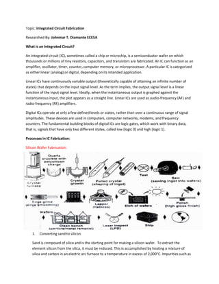
  • 1. Topic: Integrated Circuit Fabrication Researched By: Johnmar T. Diamante ECE5A What is an Integrated Circuit? An integrated circuit (IC), sometimes called a chip or microchip, is a semiconductor wafer on which thousands or millions of tiny resistors, capacitors, and transistors are fabricated. An IC can function as an amplifier, oscillator, timer, counter, computer memory, or microprocessor. A particular IC is categorized as either linear (analog) or digital, depending on its intended application. Linear ICs have continuously variable output (theoretically capable of attaining an infinite number of states) that depends on the input signal level. As the term implies, the output signal level is a linear function of the input signal level. Ideally, when the instantaneous output is graphed against the instantaneous input, the plot appears as a straight line. Linear ICs are used as audio-frequency (AF) and radio-frequency (RF) amplifiers. Digital ICs operate at only a few defined levels or states, rather than over a continuous range of signal amplitudes. These devices are used in computers, computer networks, modems, and frequency counters. The fundamental building blocks of digital ICs are logic gates, which work with binary data, that is, signals that have only two different states, called low (logic 0) and high (logic 1). Processes in IC Fabrication: Silicon Wafer Fabrication: 1. Converting sand to silicon Sand is composed of silica and is the starting point for making a silicon wafer. To extract the element silicon from the silica, it must be reduced. This is accomplished by heating a mixture of silica and carbon in an electric arc furnace to a temperature in excess of 2,000°C. Impurities such as
  • 2. iron, aluminum, boron and phosphorous also react to give their chlorides, which are then removed by fractional distillation. During the reaction, silicon is deposited on the surface of an electrically heated ultra-pure silicon rod to produce a silicon ingot. 2. Creating a cylindrical crystal To turn it into a usable material, the silicon must be turned into single crystals that have a regular atomic structure. This transformation is achieved through the Czochralski Process. Electronic-grade silicon is melted in a rotating quartz crucible and held at just above its melting point of 1,414°C. 3. Slicing the crystal into wafers Integrated circuits are approximately linear, which is to say that they're formed on the surface of the silicon. To maximize the surface area of silicon available for making chips, the silicon ingot is sliced up into discs called wafers. The wafers are just thick enough to allow them to be handled safely during semiconductor fabrication. 300mm wafers are typically 0.775mm thick. Sawing is carried out using a wire saw that cuts multiple slices simultaneously, in the same way that some kitchen gadgets cut an egg into several slices in a single operation. 4. Making a patterned oxide layer The wafer is heated to a high temperature in a furnace. The wafer is spun in a vacuum so that the photoresist spreads out evenly over the surface before being baked dry. The wafer is exposed to ultraviolet light through a photographic mask or film. The next stage is to develop the latent circuit image. The photoresist isn't sufficiently durable to withstand the hot gasses used in some steps, but it is able to withstand hydrofluoric acid, which is now used to dissolve those parts of the silicon oxide layer where the photoresist has been washed away. Finally, a solvent is used to remove the remaining photoresist, leaving a patterned oxide layer in the shape of the required circuit features. Wafer Testing: Wafer testing is a step performed during semiconductor device fabrication. During this step, performed before a wafer is sent to die preparation, all individual integrated circuits that are present on the wafer are tested for functional defects by applying special test patterns to them. The wafer testing is performed by a piece of test equipment called a wafer prober. Wafer Mounting: To facilitate the processing of the wafer at wafer saw, support is provided to the wafer by mounting the wafer on dicing tape. The dicing tape is a PVC sheet typically 3 mm in thickness with synthetic adhesive on one side to hold both the wafer frame and the wafer.
  • 3. Dicing or Wafer Sawing: Wafer saw follows wafer mounting and is the step that actually cuts the wafer into individual dice for assembly in IC packages. The wafer saw process consists of the following steps: 1. The frame-mounted wafer is automatically aligned into position for cutting; 2. The wafer is then cut thru its thickness according to the programmed die dimensions using a resin-bonded diamond wheel rotating at a very high rpm; 3. The wafer goes through a cleaning process using high pressure DI water sprayed on the rotating wafer and then dried by air-blowing. Die Bonding or Die Attach: Die Bonding is the process of attaching the silicon chip to the die pad or die cavity of the support structure of the semiconductor package. These are the two common die attach processes: 1. Adhesive Die Attach - uses adhesives such as polyimide, epoxy and silver-filled glass as die attach material to mount the die on the die pad or cavity. The adhesive is first dispensed in controlled amounts on the die pad or cavity. The die for mounting is then ejected from the wafer by one or more ejector needles. While being ejected, a pick-and-place tool commonly known as a 'collet' then retrieves the die from the wafer tape and positions it on the adhesive. 2. Eutectic Die Attach - is commonly employed in hermetic packages, uses a eutectic alloy to attach the die to the cavity. A eutectic alloy is an alloy with the lowest melting point possible for the metals combined in the alloy. The Au-Si eutectic alloy is the most commonly used die attach alloy in semiconductor packaging. Wire Bonding: Wire bonding is the process of providing electrical connection between the silicon chip and the external leads of the semiconductor device using very fine bonding wires. The wire used in wire bonding is usually made either of gold (Au) or aluminum (Al), although Cu wire bonding is starting to gain a foothold in the semiconductor manufacturing industry. These are the two common wire bonding processes: 1. Gold ball wire bonding - a gold ball is first formed by melting the end of the wire through electronic flame-off (EFO). The free-air ball is then brought into contact with the bond pad. Adequate amounts of pressure, heat, and ultrasonic forces are then applied to the ball for a specific amount of time, forming the initial metallurgical weld between the ball and the
  • 4. bond pad as well as deforming the ball bond itself into its final shape. The wire is then run to the corresponding finger of the lead frame, forming a gradual arc or "loop" between the bond pad and the lead finger. Pressure and ultrasonic forces are applied to the wire to form the second bond, this time with the lead finger. 2. Aluminum wedge wire bonding - a clamped aluminum wire is brought in contact with the aluminum bond pad. Ultrasonic energy is then applied to the wire for a specific duration while being held down by a specific amount of force, forming the first wedge bond between the wire and the bond pad. The wire is then run to the corresponding lead finger, against which it is again pressed. The second bond is again formed by applying ultrasonic energy to the wire. The wire is then broken off by clamping and movement of the wire. Molding or IC encapsulation: Molding is the process of encapsulating the device in plastic material. Transfer molding is one of the most widely used molding processes in the semiconductor industry because of its capability to mold small parts with complex features. In this process, the molding compound is first preheated prior to its loading into the molding chamber. After pre-heating, the molding compound is forced by a hydraulic plunger into the pot where it reaches melting temperature and becomes fluid. The plunger then continues to force the fluid molding compound into the runners of the mold chase. These runners serve as canals where the fluid molding compound travels until it reaches the cavities, which contain the lead frames for encapsulation. Plating or Lead Finish: Plating or Lead Finish is the process of applying a coat of metal over the leads of an IC to protect the leads against corrosion, protect the leads against abrasion, improve the solderability of the leads and improve the appearance of the leads. These are the two widely used lead finish techniques in the semiconductor industry: 1. Tin plating - is a form of pure metal electroplating, which is the process of depositing a coating of metal on a surface by passing a current through a conductive medium, or electrolyte. 2. Solder plating - is a form of alloy plating. An alloy is composed of at least two elements, at least one of which is a metal. An alloy has better properties than its component metals: it is harder, more corrosion-resistant, has better solderability and better appearance.
  • 5. Marking: Marking is the process of putting identification, traceability, and distinguishing marks on the package of an IC. The device name, company logo, date code, and lot id are examples of information commonly marked on the IC's package. Some marks are put on the package during Assembly and some marks are put on the package during Test. These are the two common marking processes: 1. Laser marking - as the name implies, refers to the process of engraving marks on the marking surface using a laser beam. There are many types of lasers, but the ones used or in use in the semiconductor industry include the CO2 laser, the YAG laser, and diode lasers. 2. Ink marking - consists of transferring an ink pattern from the plate, which is a flat block with pattern depressions that are filled with ink, to the package, using a silicone rubber stamp pad. Silicone rubber repels ink, making the transfer of the ink pattern clean and efficient. It is also resilient and elastic, making it possible to print even on uneven surfaces. Deflash/ Trim & Form /IC Singulation: Deflash - removal of flashes from the package of the newly molded parts.. Flashes are the excess plastic material sticking out of the package edges right after molding. Trim - cutting of the dambars that short the leads together. Form - forming of the leads into the correct shape and position. Singulation - cutting of the tie bars that attach the individual units to the lead frame, resulting in the individual separation of each unit from the lead frame. IC testing: In this process, the IC’s are checked by an IC tester for physical and electrical defects. Defective IC’s are retested by the previous processes to ascertain the cause of the defects.