IJERD (www.ijerd.com) International Journal of Engineering Research and Development
•
1 like•258 views

![Study of ICP-CVD grown Amorphous and Microcrystalline Silicon thin films in HIT structure
II. EXPERIMENTAL
We have used p-type 1-10 cm <100>, crystalline silicon wafer for this study. The Si films were deposited in a
planar coil ICP CVD reactor. In this system the intense degree of dissociation and ionization of silane is established in a
region away from the substrate. Silane/helium mixture passes through a distribution ring located under the plasma region.
Thus H2 is directly dissociated while silane is dissociated predominately by active particles from the plasma
4000 µc-Si peak
3500
Intensity [A.U.]
3000
a-Si:H peak
2500
2000
1500
1000
200 300 400 500 600 700 800
-1
Raman shift [cm ]
Fig.2 Raman Spectrum of μc-Si / a-Si:H sample (a-Si:H 70nm and μc-Si 20nm)
region. The process pressure for PECVD and HDPCVD are quite different. More than 100 mTorr is common for PECVD.
The pressure range of HDPCVD is 1~30 mTorr. We report on the study of 20 mTorr working pressure, 200~400℃ substrate
temperature, 200 Watt ICP power (13.56 MHz).
The high-density plasma was created by inductively coupling of RF energy to the plasma region through a silica
plate. The silica plate was vacuum jointed to the top of the reactor. All other parts of deposition chamber were made from
stainless steel. The ICP source diameter was about 20 cm. The samples were loaded on a grounded, resistance-heated stage.
The planar coil to sample distance was 10cm. Aluminium metal was deposited on the back side of the crystalline silicon
wafer using vacuum deposition technique. After rapid thermal annealing (RTA) microcrystalline silicon and hydrogenated
amorphous silicon were deposited by inductively coupled plasma chemical vapour deposition technique. Around 10 nm
thick Mg and 100 nm thick Al layer were deposited sequentially deposited and grid pattern was made by photo-lithography
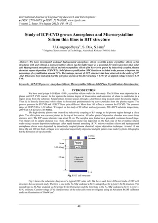
for the formation of top electrode. Fig.1 shows the schematic diagram of a typical HIT solar cell.
We have used three different kinds of HIT cell structures for our present study. The first is one is the AL/Mg/
undoped a-Si:H/ undoped c-Si/ p-type C-Si/Al structure. The second type is AL/Mg/ undoped c-Si/ p-type C-Si/Al
structure and the third type is the AL/Mg/ undoped a-Si:H/ p-type C-Si/Al structure. Current-voltage (I-V) characteristics of
the solar cells were investigated using an Advantest R6243 calibrator under an illumination of 30mW/cm2.
III. RESULT AND DISCUSSION
The material properties of thin film silicon were critically analyzed with the help of Raman Spectrum. Fig.2. shows the
Raman Spectrum of a-Si/µc-Si sample having thickness of a-Si was 70 nm and that of c-Si was 20 nm. Raman Shift peak
of c-Si at 510 cm-1 and that of a-Si at 480 cm-1 were observed. Moreover from fig. 3,
2200
a-Si:H peak at 480
Intensity [A.U.]
2000
1800
1600
200 300 400 500 600 700 800
-1
Raman shift [cm ]
Fig.3 Raman Spectrum of μc-Si / a-Si:H sample (a-Si:H 70nm and μc-Si 5nm)
we have found that the Raman peak of µc-Si/a-Si sample at 480cm-1. In this experiment, we have used a-Si thickness 70nm
and µc-Si thickness 5nm respectively. Specially, film deposited at low temperature(~2500C) followed by novel solid phase
49](data:image/gif;base64,R0lGODlhAQABAIAAAAAAAP///yH5BAEAAAAALAAAAAABAAEAAAIBRAA7)
Recommended
More Related Content
Similar to IJERD (www.ijerd.com) International Journal of Engineering Research and Development
Similar to IJERD (www.ijerd.com) International Journal of Engineering Research and Development (20)
More from IJERD Editor
More from IJERD Editor (20)
Recently uploaded
Recently uploaded (20)
IJERD (www.ijerd.com) International Journal of Engineering Research and Development
- 1. International Journal of Engineering Research and Development e-ISSN: 2278-067X, p-ISSN: 2278-800X, www.ijerd.com Volume 2, Issue 10 (August 2012), PP. 48-52 Study of ICP-CVD grown Amorphous and Microcrystalline Silicon thin films in HIT structure U.Gangopadhyay1, S. Das, S.Jana2 1,2 Meghnad Saha Institute of Technology, Nazirabad, Kolkata-700150, India Abstract––We have investigated undoped hydrogenated amorphous silicon (a-Si:H) p-type crystalline silicon (c-Si) structures with and without a microcrystalline silicon (c-Si) buffer layer as a potential for hetero-junction (HJ) solar cell. Hydrogenated amorphous silicon and microcrystalline silicon film have been grown by inductively coupled plasma chemical vapour deposition (ICP-CVD). Solid phase crystallization (SPC) has been included to the process to improve the percentage of crystallization around 72%. The leakage current of HIT structure has been observed in the order of 10-8 Amp. It has also been indicated that the activation energy of the HIT structure is 0.795 eV at applied voltage is below 0.55 Volt. Keywords––ICP-CVD process; Amorphous Silicon; Microcrystalline Silicon; Solid Phase Crystallization; Heterojunction I. INTRODUCTION We have used p-type 1-10 cm <100>, crystalline silicon wafer for this study. The Si films were deposited in a planar coil ICP CVD reactor. In this system the intense degree of dissociation and ionization of silane is established in a region away from the substrate. Silane/helium mixture passes through a distribution ring located under the plasma region. Thus H2 is directly dissociated while silane is dissociated predominately by active particles from the plasma region. The process pressure for PECVD and HDPCVD are quite different. More than 100 mTorr is common for PECVD. The pressure range of HDPCVD is 1~30 mTorr. We report on the study of 20 mTorr working pressure, 200~400℃ substrate temperature, 200 Watt ICP power (13.56 MHz). The high-density plasma was created by inductively coupling of RF energy to the plasma region through a silica plate. The silica plate was vacuum jointed to the top of the reactor. All other parts of deposition chamber were made from stainless steel. The ICP source diameter was about 20 cm. The samples were loaded on a grounded, resistance-heated stage. The planar coil to sample distance was 10cm. Aluminium metal was deposited on the back side of the crystalline silicon wafer using vacuum deposition technique. After rapid thermal annealing (RTA) microcrystalline silicon and hydrogenated amorphous silicon were deposited by inductively coupled plasma chemical vapour deposition technique. Around 10 nm thick Mg and 100 nm thick Al layer were deposited sequentially deposited and grid pattern was made by photo-lithography for the formation of top electrode. Fig.1 HIT cell structure Fig.1 shows the schematic diagram of a typical HIT solar cell. We have used three different kinds of HIT cell structures for our present study. The first is one is the AL/Mg/ undoped a-Si:H/ undoped c-Si/ p-type C-Si/Al structure. The second type is AL/Mg/ undoped c-Si/ p-type C-Si/Al structure and the third type is the AL/Mg/ undoped a-Si:H/ p-type C- Si/Al structure. Current-voltage (I-V) characteristics of the solar cells were investigated using an Advantest R6243 calibrator under an illumination of 30mW/cm2. 48
- 2. Study of ICP-CVD grown Amorphous and Microcrystalline Silicon thin films in HIT structure II. EXPERIMENTAL We have used p-type 1-10 cm <100>, crystalline silicon wafer for this study. The Si films were deposited in a planar coil ICP CVD reactor. In this system the intense degree of dissociation and ionization of silane is established in a region away from the substrate. Silane/helium mixture passes through a distribution ring located under the plasma region. Thus H2 is directly dissociated while silane is dissociated predominately by active particles from the plasma 4000 µc-Si peak 3500 Intensity [A.U.] 3000 a-Si:H peak 2500 2000 1500 1000 200 300 400 500 600 700 800 -1 Raman shift [cm ] Fig.2 Raman Spectrum of μc-Si / a-Si:H sample (a-Si:H 70nm and μc-Si 20nm) region. The process pressure for PECVD and HDPCVD are quite different. More than 100 mTorr is common for PECVD. The pressure range of HDPCVD is 1~30 mTorr. We report on the study of 20 mTorr working pressure, 200~400℃ substrate temperature, 200 Watt ICP power (13.56 MHz). The high-density plasma was created by inductively coupling of RF energy to the plasma region through a silica plate. The silica plate was vacuum jointed to the top of the reactor. All other parts of deposition chamber were made from stainless steel. The ICP source diameter was about 20 cm. The samples were loaded on a grounded, resistance-heated stage. The planar coil to sample distance was 10cm. Aluminium metal was deposited on the back side of the crystalline silicon wafer using vacuum deposition technique. After rapid thermal annealing (RTA) microcrystalline silicon and hydrogenated amorphous silicon were deposited by inductively coupled plasma chemical vapour deposition technique. Around 10 nm thick Mg and 100 nm thick Al layer were deposited sequentially deposited and grid pattern was made by photo-lithography for the formation of top electrode. Fig.1 shows the schematic diagram of a typical HIT solar cell. We have used three different kinds of HIT cell structures for our present study. The first is one is the AL/Mg/ undoped a-Si:H/ undoped c-Si/ p-type C-Si/Al structure. The second type is AL/Mg/ undoped c-Si/ p-type C-Si/Al structure and the third type is the AL/Mg/ undoped a-Si:H/ p-type C-Si/Al structure. Current-voltage (I-V) characteristics of the solar cells were investigated using an Advantest R6243 calibrator under an illumination of 30mW/cm2. III. RESULT AND DISCUSSION The material properties of thin film silicon were critically analyzed with the help of Raman Spectrum. Fig.2. shows the Raman Spectrum of a-Si/µc-Si sample having thickness of a-Si was 70 nm and that of c-Si was 20 nm. Raman Shift peak of c-Si at 510 cm-1 and that of a-Si at 480 cm-1 were observed. Moreover from fig. 3, 2200 a-Si:H peak at 480 Intensity [A.U.] 2000 1800 1600 200 300 400 500 600 700 800 -1 Raman shift [cm ] Fig.3 Raman Spectrum of μc-Si / a-Si:H sample (a-Si:H 70nm and μc-Si 5nm) we have found that the Raman peak of µc-Si/a-Si sample at 480cm-1. In this experiment, we have used a-Si thickness 70nm and µc-Si thickness 5nm respectively. Specially, film deposited at low temperature(~2500C) followed by novel solid phase 49
- 3. Study of ICP-CVD grown Amorphous and Microcrystalline Silicon thin films in HIT structure crystallization(SPC) showed a crystalline peak at around 510cm-1,showing that this film has a microcrystalline phase in an amorphous matrix. Table-1: Crystalinity value of different samples Substrate RF power in Watt Crystalinity % temperature(oC) 250 200 67 50 300 67 250 400 70 250 500 72 Table 1 shows the crystallized volume fraction of different experimental samples under different RF power for substrate temperature at 2500C. It was extracted from the equation /[ +0.8(1-),where is the fraction of the crystalline integrated intensity Ic/(Ic+IA).Here Ic represents the integrated intensity under the crystalline peak and IAis the integrated contribution from the amorphous phase[12].The maximum crystallization of 72% was achieved at RF power 500watt. High value of crystalinity helps to increase the photoconductivity value. 0 10 -1 10 -2 10 -3 10 Log I(A) -4 10 a-Si / uc-Si = 700 / 50 -5 10 -6 10 a-Si / uc-Si = 700 / 400 -7 10 a-Si / uc-Si = 700 / 200 -8 10 -9 10 -3 -2 -1 0 1 2 3 Voltage(V) Fig.4 I-V Characteristic of a-Si:H /μc-Si HIT Cell Fig.4 shows the I-V characteristics of the a-Si/µc-Si HIT type cells. This cell with 20nm thick µc-Si has a leakage current in order of 10-8Amp. Fig.5 shows the J-V-T characteristics of the a-Si/µc-Si HIT having thickness 70nm of a-Si film and 5nm ofµc-Si film respectively. The expressions J=Joexp(AV) and Jexp(-Ea/kT) were used for calculation of the activation energies of electron. Using Fig.6, the calculated activation energy was found 0.795eV. 1 10 0 10 -1 Current density [A/cm ] 10 2 -2 10 -3 10 -4 10 -5 10 -6 200K 10 -7 225K 10 -8 250K 10 275K -9 10 300K -10 H325K 10 -11 H350K 10 -12 10 -3 -2 -1 0 1 2 3 Voltage [V] Fig.5 J-V-T Characteristic of a-Si:H /μc-Si HIT cell at V<0.5V 50
- 4. Study of ICP-CVD grown Amorphous and Microcrystalline Silicon thin films in HIT structure -10 Ea = 0.795 eV -12 -14 -16 ln(Jo) -18 -20 -22 -24 -26 35 40 45 50 55 60 -1 1/kT [eV ] Fig.6 Temperature dependence of Jo of the heterojunction when 0.3<V<0.50 The J-V-T plots as shown in Fig.5 generally show a slope change at around V=0.5V, meaning that a different conduction mechanism start to dominate from this voltage until the conduction become spacecharge limited when V>0.5V. In addition, the relatively constant slope throughout this temperature range means that A is almost temperature independent as illustrated in Fig.5 for 0.3<V<0.5V. This behavior is typical of the temperature independent conduction mechanism of tunnelling [13].Among various tunneling mechanism, the conduction seems to follow the MTCE model, which is widely believed to be one of the dominant conduction mechanism in a-Si:H/c-Si heterojunctions. This is reasonably explained by both the increased probability of multistep tunnelling, resulting from the continuously distributed localized states within in the band gap of a-Si:H (or µc-Si ) and the linear relationship between logJ0 and 1/kT as shown in Fig. 6. 0 10 uc-Si/a-Si = 700/50 -1 10 uc-Si/a-Si = 700/200 -2 uc-Si/a-Si = 700/400 10 -3 10 Log I(A) -4 10 -5 10 -6 10 -7 10 -8 10 -9 10 -3 -2 -1 0 1 2 3 Voltage(V) Fig.7 I-V Characteristic of a-Si:H of HIT cell Fig.7 shows the I-V characteristics of a-Si HIT cell. From this figure the leakage current 50nm a-Si HIT was found as 2×10⁻⁷Amp. Fig.8 shows the I-V characteristics of µc-Si /a-Si HIT. Type cell having 10-8Amp. leakage current. This implies that the thickness of a-Si layer does not have any effect on the leakage current. 51
- 5. Study of ICP-CVD grown Amorphous and Microcrystalline Silicon thin films in HIT structure 0 10 uc-Si/a-Si = 700/50 -1 10 uc-Si/a-Si = 700/200 -2 uc-Si/a-Si = 700/400 10 -3 10 Log I(A) -4 10 -5 10 -6 10 -7 10 -8 10 -9 10 -3 -2 -1 0 1 2 3 Voltage(V) Fig.8 I-V Characteristic of μc-Si / a-Si:H HIT cell IV. CONCLUSION In this paper, the feature of the HIT (heterojunction with Intrinsic thin layer) structure are reviewed. Around 72% crystalinity value of the µc-Si film has been achieved using solid phase crystallization (SPC) method. The HIT Solar cell depicts a simple structure and a low processing temperature (2500C). The leakage current is in the order of 10-8Amp. in I-V Characteristic of the HIT type cells. Hit cell activation energy is determined as 0.795eV when the applied voltage is below 0.5V. V. ACKNOWLEDGEMENTS The authors deeply acknowledge Meghnad Saha Institute of Technology, TIG provides the infrastructural support for carrying out research activity in this area. The authors also gratefully to acknowledge the DST, Govt. of India for financial support for carrying out solar cell related research activity. REFERENCES [1]. W.A.Anderson, B.Jagannathan and E.Klementieva, “Lightweight, thin-film Si Heterojunction solar cells”, Progress in Photovoltaics 5 (1997)433 [2]. B.Jagannathan, W.A. Anderson and J.Coleman, "Amorphous-Silicon P-Type Crystalline Silicon Heterojunction Solar-Cells”, Solar Energy Mat, and Solar cells 46(1997) 289. [3]. R.Stangl, A.Froitzheim, W.Fuhs, “Thin Film Silicon Emitters For Crystalline Silicon Solar Cells, Epitaxial, Amorphous or Microcrystalline? - A Simulation Study “European PV Conference, Rome, Oct.2002, 1-4. [4]. T.H. Wang, E. Iwaniczko, M.R. Page, D.H. Levi, Y. Yan,” Effective Interfaces in Silicon Heterojunction Solar Cells” Proc. of IEEE PV conference (2005),p955 [5]. M.W.M.van Cleef, F.A. Rubinelli and R.E.I Schropp, Proc. of 14thEuropean Photovoltaic Solar Energy Conference and Exhibition, Barocelona, Spain (1997) p 50 [6]. B.Jagannathan, and W.A.Anderson, “Interface effects on the carrier transport and photovoltaic properties of hydrogenated amorphous silicon/crystalline silicon solar cells” “Solar Energy Mat. And Solar cells, 44 (1996) 165 [7]. M.W.M. Van Cleef, F.A.R.E.I. Schropp, Mat. Res. Soc. Symp. Proc. 507 (1998) p125 [8]. P. Brogueira, S.Grebner, F.Wang, R.Schwarz,V.Chu and J.P.Conde, Mat. Res. Soc. Symp. Proc.297 (1998)p121 [9]. F.Finger, P.Hapke, M.Luysberg, R.Carius,H.Wagner and M .Scheib, “Improvement of grain size and deposition rate of microcrystalline silicon by use of very high frequency glow discharge” Appl. Phys. Lett. 65(1994) 2588 [10]. M.Kitagawa, S.Ishihara, K.Setsune, Y.Manabe, and T.Hirao,“Low Temperature Preparation of Hydrogenated Amorphous Silicon by Microwave Electron-Cyclotron-Resonance Plasma CVD” Jpn. J. Appl. Phys. 26(1987)L231 [11]. Byeong Yeon Moon, Jae Hyoung Youn, Sung Hwan Won,Jin Jang, Polycrystalline silicon film deposited by ICP-CVD, Solar energy Mat. and Solar cells 69(2001)139-145. [12]. Vivek Subramanian, Paul Dankoski, Levent Degertekin, Butrus T.Khuri-Yakub, and Krishna C.Saraswat, “Controlled Two- Step Solid- Phase Crystallization for High-Performance Polysilicon TFT’s”, IEEE Electron Devices Letters, Vol. 18, 8 (1997)378-381 [13]. B. Jagannathan, R. L. Wallace, and W. A. Anderson , “Structural and electrical properties of thin microcrystalline silicon films deposited by an electron cyclotron resonance plasma discharge of 2% SiH4/Ar further diluted in H2””, J. Vac. Sci. Technol. A 16, 2751 (1998). [14]. H. Matsuura, T.Okuno, H. Okushi, and K.Tanaka, “Electrical properties of n‐amorphous/p‐crystalline silicon heterojunctions” J. Appl. Phys. 55, 1012 (1984 52