SlideShare uma empresa Scribd logo
1 de 4
Baixar para ler offline
P R O D U C T U P D AT E


HIGH PERFORMANCE DEVICE GENERATION

New Approach to Accelerating Analog Layout Surpasses
Full Custom and Traditional Automation Methodologies
Despite many efforts to automate analog design and layout, these          approach among members also drives up the time required for the
tasks remain primarily a full custom process, with the result that        review process and increases the risk of needing additional design
analog is occupying a larger and larger portion of the total design       spins. These problems appear most often in the more difficult
cycle time. Efforts to automate analog design have not been               areas of high speed, low noise, high precision analog design where
successful in the marketplace because the tools have not been             device matching is critical to performance. Expertise even in basic
able to equal the quality levels of full custom design, are complex       matching techniques can vary from engineer to engineer, which
to set up and use, and are expensive.                                     can in some cases lead to the chip failing. Layout engineers with
                                                                          the experience and knowledge to go beyond the basic techniques
Tanner EDA’s new tool forgoes full automation in favor of                 produce designs that are much more likely to work the first time,
accelerating the layout process by generating key analog design           but such people are in short supply. A leading analog foundry
primitives, such as current mirrors and differential pairs. These         recently cited matching issues as the single biggest cause of re–
primitives are often the most time–consuming aspect of layout and         spins in their customer’s designs.
indeed the parts that are critical to the functionality of the silicon.
The new tool applies matching techniques to address common
processing artifacts, produces the optimal solution for parasitics
and silicon area, and creates devices optimized for high yield.

Layout engineers maintain complete freedom to manually place
and route these structures as well as being able to tune the output
to their specific requirements. Surpassing traditional automation
methodologies, this new layout approach dramatically improves
layout productivity and reduces design cycle times while generating
structures at a level of quality that consistently matches that of the
most experienced layout engineers.

Analog layout is becoming the primary bottleneck in
the design process
Analog layout has traditionally been considered to be more
challenging than digital layout. For example, it takes considerably
more time to achieve a high level of expertise in analog layout                Figure 1: Transistor count vs. time to GDSII by Technology Node
as compared to the time required to master digital layout. So it          As process technology moves deep into the nanometer realm, the
comes as no surprise that digital design automation technology            impact of process variations and parasitic effects have caused the
has advanced at a much faster pace than its analog counterpart.           analog layout process to be highly iterative and time–consuming.
Since digital occupies the vast majority of most projects, design         Analog layouts often must be revised, re–simulated and the results
cycle times have trended downwards even as transistor counts              evaluated over and over again to achieve a robust solution. In a
have continued to increase geometrically.                                 typical project, analog may occupy only a small portion of the silicon
Right now, most analog layout engineers use either a full custom          area but can consume a very large portion of the layout effort. As
approach—drawing every polygon—or use basic device generators             feature sizes are reduced, the time required for full custom analog
provided by the foundry to create MOSFETs, capacitors, resistors,         layout is rising, with the result that many companies are seeing an
etc. The vast majority of layout engineers manually place these           increase in time–to–GDSII at nanometer technology nodes. Figure
devices together to form basic analog structures such as current          1 shows data collected from a sampling of customers of IC Mask
mirrors and differential pairs, which in turn are connected together      Design, a company that provides analog physical design services.
to form the overall circuit. The quality of the resulting layout is
obviously heavily dependent upon the expertise of the individual          Existing analog automation solutions have not gained
layout engineer.                                                          acceptance by users
The very long period of time required to develop expertise                Large and small vendors offer varying approaches to analog
in analog layout means that skill levels vary widely among the            automation, ranging from simple device generation tools to full–
members of the typical layout team. The lack of a consistent              blown analog layout automation. One analog automation solution
focuses on providing advanced editing features for creating and
editing parameterized cells to expedite the process of creating
matched structures. Another tool builds on the parameterized cell
approach by adding many additional parameters and technology
independence. Both operate only at the device level, so they
do not address the layout of circuits and structures, which is not
only the most time–consuming part of the analog layout process,
but also the portion that is most prone to poor quality and
inconsistency. Large amounts of time are required to generate
individual structures by hand and the quality of the resulting layout
varies depending upon the skill of the individual engineer.

Another analog layout solution attempts to completely automate
the analog layout process. It provides a programming language
that allows users to code their own physical cells and its placement
engine generates the layout based on these cells. But the coding
takes place at a high level that does not take into consideration
the basic characteristics of the key building blocks and may not lay
                                                                                   Figure 2: Generation of structures based on existing DRC rules
them out with the correct considerations. Users often find that the
resulting designs do not compare in quality to a manually created
                                                                             Retargeting the components to a new technology node simply
layout. Yet another tool takes as input a set of design rules and
                                                                             requires the user to input the manufacturing rules for that
then generates basic structures, which are also placed and routed.
                                                                             technology and regenerate the devices and primitives. So it is
One weakness of this approach is that it applies global matching
                                                                             possible to very quickly move a design to a new technology node
rules to the entire layout while skilled manual designers understand
                                                                             or to a different foundry.
that a current mirror, for example, should not be laid out in the
same way as a differential pair. One more obstacle to adoption is            HiPer DevGen was designed to be implemented with little or no
its list price, which is quoted at close to a million dollars for a single   change to existing design flows. Unlike existing full automation
license.                                                                     tools, it works with unmodified schematics. It also uses as input
                                                                             netlists produced for schematic driven layout (SDL) and also accepts
Tanner EDA’s HiPer DevGen (High Performance Device                           input directly from S-Edit, Tanner EDA’s schematic editor. HiPer
Generator) accelerates analog layout by automatically                        DevGen builds upon Tanner EDA’s existing T-Cell architecture of
generating common structures                                                 parameterized cells that exist within the company’s L-Edit layout
                                                                             editor. The generated cells are cached in the database for maximum
As we’ve seen above, previous methods to try to automate the                 performance. HiPer DevGen automatically recognizes the building
analog design process have been primarily based either at the cell           blocks of the design and generates technology–aware building
level or at the level of the complete design. A new approach is              blocks. The layout engineer then connects the blocks together and
based on accelerating analog layout by generating primitives that            wires them to pins to complete the design.
are used over and over again such as current mirrors, differential
pairs and resistor dividers. This approach creates these building
blocks based on an understanding of the functional requirements              Quality equals that which can be achieved by best
that are needed to produce a high–quality layout. Rather than                analog layout engineers
attempting to completely automate analog design, HiPer DevGen                The HiPer DevGen generation engine is “silicon–aware” and
accelerates the most time–consuming aspects of the layout                    produces devices that are optimized for high yield, including
process to substantially reduce the amount of time required for              double contacts and vias and support for design for manufacturing
analog layout while improving quality and design consistency.                (DFM ) rules, where applicable. The generation engine takes into
                                                                             account over 20 common processing artifacts and applies matching
By automatically generating the layout of devices—including
                                                                             techniques so that these processing effects are reduced where
MOS transistors and resistors as well as MOS current mirrors, MOS
                                                                             possible or are applied equally across all matched devices. These
differential pairs, resistor dividers and other basic structures—this
                                                                             artifacts include, but are not limited to:
new approach provides nearly the same degree of acceleration as
full automation, but with higher quality. As well as automating the          » Linear process gradients
tedious, repetitive aspects of the design process, HiPer DevGen
also eliminates the complex and often very expensive setup                   » Mask misalignment
process that is required with current analog automation tools.               » Implant shadowing
HiPer DevGen automatically generates both devices and analog                 » Photolithographic invariance
design primitives using only the manufacturing design rules for the
specific technology node as its input. The tool itself understands           » Current flow direction
the technology and matching requirements and automatically                   » Mechanical stress, including shallow trench isolation (STI )
generates the basic building blocks of analog layout with these                or length of diffusion (LOD )
requirements taken into account. Layout engineers have complete
freedom to lay out and place and route these structures. HiPer               » Antenna effect/Vt shift
DevGen is provided with basic default values that meet the
requirements of 90% of analog designs. For example, in a differential
                                                                             » Well proximity effect (WPE)
pair it will always attempt to optimize the drain parasitics over the        HiPer DevGen ensures a consistent and high quality approach to
source parasitics. However in circuits such as down mixers, where            the layout of complex analog structures across layout engineers,
the source capacitance is more critical, the designer or layout              design teams and engineering sites. The generation engine
engineer can easily change these parameters, regenerate, simulate            considers device and interconnect parasitics and silicon area,
the design and converge on an optimal design approach.                       and produces the optimal solution based on design inputs,
foundry manufacturing rules, and user matching requirements.             Figure 4 shows a more complex current mirror, again with dummies,
Matching, parasitic, and performance considerations are tuned            but in this case there are three output currents. In this case they
to specific analog structures such as the previously mentioned           are being scaled by two, two, and four respectively. This structure
differences between current mirrors and differential pairs. The          would take considerably longer than the first example (Figure 1)
generation engine understands the key parameters associated              if done by hand and its complexity increases the possibility of an
with each structure and generates the structures so that these           error that could cause rework or quality problems. HiPer DevGen
key requirements are met while maintaining a continual focus on          also generated this device instantly, with only the manufacturing
silicon quality, yield, silicon performance, and matching.               rules provided as input.

The generation engine also can be adjusted to ensure that its
output fits the user’s specific matching, parasitic, and performance
requirements. For example, HiPer DevGen offers the user the ability
to prioritize parasitic performance over matching requirements or
vice versa, and also gives precedence to key matching concerns
over others within a circuit. For instance on large devices, where a
mismatch due to linear gradients is recognized as being a priority,
the generation of the structure can be weighted towards that, as
opposed to a possible mismatch in drain or source area.

Examples of how this approach works in practice


                                                                                       Figure 5: Two finger differential pair.
                                                                         Figure 5 shows a simple two fingered differential pair with a guard
                                                                         ring. In this case, the drain capacitance is optimized on both
                                                                         devices and the gates are densely connected in metal in order to
                                                                         reduce gate resistance and lower parasitic channel noise. While
                                                                         this example consists of only two transistors with two fingers each,
                                                                         the care required to lay out the structure increases the layout time
                                                                         dramatically. In conjunction with the increased layout effort, the risk
                                                                         of laying it out incorrectly, such as by optimizing the drain, also
                                                                         increases and these errors are typically only spotted either in silicon
                                                                         or where design flows ensure stringent extraction and post–layout
                  Figure 3: Example current mirror                       simulation of all circuits. With HiPer DevGen, it is possible to create
                                                                         this instantly and, if necessary, generate multiple variants, allowing
An example of a current mirror is shown in Figure 3. While an            circuit designers to simulate each solution and converge on an
experienced layout engineer would probably spend only a short            optimal solution for their design in the shortest period of time.
time to create this structure, the possibility exists that he or she
might make an error that could take hours or even days to resolve
later in the design cycle. Worse still, such as error could produce a
circuit that is LVS and DRC–clean by construction, but has a mismatch,
resulting in the problem only being seen in silicon. HiPer DevGen
instantly created the structure shown, with the added assurance
that it meets all requirements of the targeted technology.


                                                                                          Figure 6: Eight finger differential pair

                                                                         Figure 6 shows a more complex differential pair with two devices
                                                                         of eight fingers each as well as a guard ring, protection diodes,
                                                                         and dummy devices. In this case, the capacitance of the source
                                                                         also is being optimized. A device of this complexity would take
                                                                         considerably more time than the previous example to lay out by
            Figure 4: Complex current mirror with dummies                hand. Manual layout would also present considerable risk of error.
For example, moving one of these devices by a micron could                A number of analog layout engineers were asked how long it would
introduce a mismatch into the device. HiPer DevGen instantly              take them to lay out this circuit, while obeying best layout practice
generated this device while simultaneously providing perfect              and applying common matching techniques. Their answers ranged
matching between both devices.                                            from two hours to two days with an average time of approximately
                                                                          five hours. The complexity of the design means that nearly every
                                                                          engineer would do it differently and these differences have the
                                                                          potential, at best, to lengthen the review process or, at worst, to
                                                                          create yield problems or indeed non–functioning silicon. On the
                                                                          other hand, using HiPer DevGen, a layout engineer instantaneously
                                                                          generated all of the individual structures in the circuit, significantly
                                                                          reducing the overall design effort. The layout engineer then
                                                                          manually floorplanned the circuit and completed the interconnect
                                                                          between devices. Each device or structure was created exactly
                                                                          the same to meet all requirements of the technology, correct by
                                                                          construction in terms of passing layout versus. schematic checks
                                                                          (LVS ), DRC clean and with guaranteed matching.

                                                                          Using this approach, let’s suppose that the designer changes a
                                                                          parameter, such as increasing the number of fingers or making
                                                                          the block shorter or wider to fit a different floor plan. Or maybe
                                                                          multiple configurations are required to address parasitics
    Figure 7: Schematic of example circuit with 17 functional devices     identified during simulation. If the design were done by hand,
                                                                          alternate versions would probably take just as long as the first
                                                                          version to lay out, consuming additional hours or days. With HiPer
                                                                          DevGen, the layout engineer can simply change a parameter and
                                                                          regenerate the structures that make up the design, completing
                                                                          the modifications in a matter of minutes. This acceleration in the
                                                                          design process makes it possible to reduce design cycle time by
                                                                          designing multiple parallel paths to see which one is best for any
                                                                          given circuit. For example, you might evaluate the ability of several
                                                                          different design alternatives to simulate the effects of artifacts such
                                                                          as LOD/STI or WPE.

                                                                          Conclusion
                                                                          HiPer DevGen increases analog layout productivity by accelerating
                                                                          the generation of devices and common analog structures. All cells
                                                                          are generated at a consistently high level of quality. Silicon quality,
                                                                          yield, silicon performance, and matching are as good as the best
                                                                          full custom layout engineer could produce and well above current
                                                                          fully automated layout generation. Design standards are the same
      Figure 8: Layout of example circuit with 17 functional devices      for different designers and different projects. Re–targeting to new
                                                                          technology nodes is effortless.
Figures 7 & 8 show a complete circuit. The top row of four transistors
(two fingers in each device) is made up of two current mirrors, the
next row of four transistors (two fingers in each device) is made up
of two differential pairs and the bottom row of three transistors
is another current mirror, comprising five gates in total. While not
shown in the schematic, approximately ten dummy devices would
also be required in order to ensure matching, bringing the total
device count from seventeen to twenty–seven.

                                        Find out how HiPer DevGen can accelerate your analog layout design.
                                      Contact us at AnalogLayout@tannereda.com to schedule your evaluation.

About Tanner EDA

Tanner EDA provides of a complete line of software solutions that catalyze innovation for the
design, layout and verification of analog and mixed-signal (A/MS) integrated circuits (ICs).
                                                                                                               Corporate Headquarters
Customers are creating breakthrough applications in areas such as power management, displays                   825 South Myrtle Avenue
and imaging, automotive, consumer electronics, life sciences, and RF devices. A low learning                   Monrovia, CA 91016-3424 USA
curve, high interoperability, and a powerful user interface improve design team productivity and               Tel: +1-626-471-9700
enable a low total cost of ownership (TCO). Capability and performance are matched by low                      Toll Free: 877-325-2223
support requirements and high support capability as well as an ecosystem of partners that bring                Fax: +1-626-471-9800
                                                                                                               Email: sales@tannereda.com
advanced capabilities to A/MS designs.
                                                                                                               Web: www.TannerEDA.com
Founded in 1988, Tanner EDA solutions deliver the right mixture of features, functionality and
                                                                                                               © 2010 Tanner Research. All rights reserved.
usability. The company has shipped over 33,000 licenses of its software to more than 5,000                     All other company and/or product names are the
customers in 67 countries.                                                                                     property of their respective owners.

Mais conteúdo relacionado

Destaque

Tweview Brandwatch Talk
Tweview Brandwatch TalkTweview Brandwatch Talk
Tweview Brandwatch TalkCoup Media
 
Q Ladilla
Q LadillaQ Ladilla
Q Ladillacaracha
 
Strategic leadership
Strategic leadershipStrategic leadership
Strategic leadershipYayvo.com
 
Interview questions
Interview questionsInterview questions
Interview questionsYayvo.com
 
Introduction to Coup Media
Introduction to Coup MediaIntroduction to Coup Media
Introduction to Coup MediaCoup Media
 
¿Por qué hay canciones que se quedan grabadas en la cabeza? Manuel Mustafa
¿Por qué hay canciones que se quedan grabadas en la cabeza? Manuel Mustafa¿Por qué hay canciones que se quedan grabadas en la cabeza? Manuel Mustafa
¿Por qué hay canciones que se quedan grabadas en la cabeza? Manuel MustafaManuel Mustafa
 
The changing role of human resource function
The changing role of human resource functionThe changing role of human resource function
The changing role of human resource functionAlexel Limited
 
Rozee.pk Top Employer Rankings 2013
Rozee.pk Top Employer Rankings 2013Rozee.pk Top Employer Rankings 2013
Rozee.pk Top Employer Rankings 2013Yayvo.com
 
Attributes of an effective Call Center Executive
Attributes of an effective Call Center ExecutiveAttributes of an effective Call Center Executive
Attributes of an effective Call Center ExecutiveYayvo.com
 
Innovation & New Venture Creation
Innovation & New Venture CreationInnovation & New Venture Creation
Innovation & New Venture CreationYayvo.com
 
2011 data quality challenges when implementing classroom value added models
2011 data quality challenges when implementing classroom value added models2011 data quality challenges when implementing classroom value added models
2011 data quality challenges when implementing classroom value added modelsChristopher Thorn
 
Hodgson Consulting Scope of Solutions
Hodgson Consulting Scope of SolutionsHodgson Consulting Scope of Solutions
Hodgson Consulting Scope of Solutionstmurad
 
غابرييل غارسيا ماركيز - مئة عام من العزلة - رواية
غابرييل غارسيا ماركيز - مئة عام من العزلة - روايةغابرييل غارسيا ماركيز - مئة عام من العزلة - رواية
غابرييل غارسيا ماركيز - مئة عام من العزلة - روايةAli Alaaraj
 

Destaque (16)

Tweview Brandwatch Talk
Tweview Brandwatch TalkTweview Brandwatch Talk
Tweview Brandwatch Talk
 
Q Ladilla
Q LadillaQ Ladilla
Q Ladilla
 
C Aracas
C AracasC Aracas
C Aracas
 
Strategic leadership
Strategic leadershipStrategic leadership
Strategic leadership
 
Interview questions
Interview questionsInterview questions
Interview questions
 
Introduction to Coup Media
Introduction to Coup MediaIntroduction to Coup Media
Introduction to Coup Media
 
¿Por qué hay canciones que se quedan grabadas en la cabeza? Manuel Mustafa
¿Por qué hay canciones que se quedan grabadas en la cabeza? Manuel Mustafa¿Por qué hay canciones que se quedan grabadas en la cabeza? Manuel Mustafa
¿Por qué hay canciones que se quedan grabadas en la cabeza? Manuel Mustafa
 
The changing role of human resource function
The changing role of human resource functionThe changing role of human resource function
The changing role of human resource function
 
Rozee.pk Top Employer Rankings 2013
Rozee.pk Top Employer Rankings 2013Rozee.pk Top Employer Rankings 2013
Rozee.pk Top Employer Rankings 2013
 
Attributes of an effective Call Center Executive
Attributes of an effective Call Center ExecutiveAttributes of an effective Call Center Executive
Attributes of an effective Call Center Executive
 
Innovation & New Venture Creation
Innovation & New Venture CreationInnovation & New Venture Creation
Innovation & New Venture Creation
 
2011 data quality challenges when implementing classroom value added models
2011 data quality challenges when implementing classroom value added models2011 data quality challenges when implementing classroom value added models
2011 data quality challenges when implementing classroom value added models
 
Hodgson Consulting Scope of Solutions
Hodgson Consulting Scope of SolutionsHodgson Consulting Scope of Solutions
Hodgson Consulting Scope of Solutions
 
Incident Command Vehicles
Incident Command VehiclesIncident Command Vehicles
Incident Command Vehicles
 
Library Sources
Library SourcesLibrary Sources
Library Sources
 
غابرييل غارسيا ماركيز - مئة عام من العزلة - رواية
غابرييل غارسيا ماركيز - مئة عام من العزلة - روايةغابرييل غارسيا ماركيز - مئة عام من العزلة - رواية
غابرييل غارسيا ماركيز - مئة عام من العزلة - رواية
 

Último

What is DBT - The Ultimate Data Build Tool.pdf
What is DBT - The Ultimate Data Build Tool.pdfWhat is DBT - The Ultimate Data Build Tool.pdf
What is DBT - The Ultimate Data Build Tool.pdfMounikaPolabathina
 
Arizona Broadband Policy Past, Present, and Future Presentation 3/25/24
Arizona Broadband Policy Past, Present, and Future Presentation 3/25/24Arizona Broadband Policy Past, Present, and Future Presentation 3/25/24
Arizona Broadband Policy Past, Present, and Future Presentation 3/25/24Mark Goldstein
 
Unleashing Real-time Insights with ClickHouse_ Navigating the Landscape in 20...
Unleashing Real-time Insights with ClickHouse_ Navigating the Landscape in 20...Unleashing Real-time Insights with ClickHouse_ Navigating the Landscape in 20...
Unleashing Real-time Insights with ClickHouse_ Navigating the Landscape in 20...Alkin Tezuysal
 
Passkey Providers and Enabling Portability: FIDO Paris Seminar.pptx
Passkey Providers and Enabling Portability: FIDO Paris Seminar.pptxPasskey Providers and Enabling Portability: FIDO Paris Seminar.pptx
Passkey Providers and Enabling Portability: FIDO Paris Seminar.pptxLoriGlavin3
 
From Family Reminiscence to Scholarly Archive .
From Family Reminiscence to Scholarly Archive .From Family Reminiscence to Scholarly Archive .
From Family Reminiscence to Scholarly Archive .Alan Dix
 
Merck Moving Beyond Passwords: FIDO Paris Seminar.pptx
Merck Moving Beyond Passwords: FIDO Paris Seminar.pptxMerck Moving Beyond Passwords: FIDO Paris Seminar.pptx
Merck Moving Beyond Passwords: FIDO Paris Seminar.pptxLoriGlavin3
 
The Ultimate Guide to Choosing WordPress Pros and Cons
The Ultimate Guide to Choosing WordPress Pros and ConsThe Ultimate Guide to Choosing WordPress Pros and Cons
The Ultimate Guide to Choosing WordPress Pros and ConsPixlogix Infotech
 
Take control of your SAP testing with UiPath Test Suite
Take control of your SAP testing with UiPath Test SuiteTake control of your SAP testing with UiPath Test Suite
Take control of your SAP testing with UiPath Test SuiteDianaGray10
 
A Journey Into the Emotions of Software Developers
A Journey Into the Emotions of Software DevelopersA Journey Into the Emotions of Software Developers
A Journey Into the Emotions of Software DevelopersNicole Novielli
 
Moving Beyond Passwords: FIDO Paris Seminar.pdf
Moving Beyond Passwords: FIDO Paris Seminar.pdfMoving Beyond Passwords: FIDO Paris Seminar.pdf
Moving Beyond Passwords: FIDO Paris Seminar.pdfLoriGlavin3
 
Decarbonising Buildings: Making a net-zero built environment a reality
Decarbonising Buildings: Making a net-zero built environment a realityDecarbonising Buildings: Making a net-zero built environment a reality
Decarbonising Buildings: Making a net-zero built environment a realityIES VE
 
Genislab builds better products and faster go-to-market with Lean project man...
Genislab builds better products and faster go-to-market with Lean project man...Genislab builds better products and faster go-to-market with Lean project man...
Genislab builds better products and faster go-to-market with Lean project man...Farhan Tariq
 
The Future Roadmap for the Composable Data Stack - Wes McKinney - Data Counci...
The Future Roadmap for the Composable Data Stack - Wes McKinney - Data Counci...The Future Roadmap for the Composable Data Stack - Wes McKinney - Data Counci...
The Future Roadmap for the Composable Data Stack - Wes McKinney - Data Counci...Wes McKinney
 
DevEX - reference for building teams, processes, and platforms
DevEX - reference for building teams, processes, and platformsDevEX - reference for building teams, processes, and platforms
DevEX - reference for building teams, processes, and platformsSergiu Bodiu
 
How to Effectively Monitor SD-WAN and SASE Environments with ThousandEyes
How to Effectively Monitor SD-WAN and SASE Environments with ThousandEyesHow to Effectively Monitor SD-WAN and SASE Environments with ThousandEyes
How to Effectively Monitor SD-WAN and SASE Environments with ThousandEyesThousandEyes
 
2024 April Patch Tuesday
2024 April Patch Tuesday2024 April Patch Tuesday
2024 April Patch TuesdayIvanti
 
UiPath Community: Communication Mining from Zero to Hero
UiPath Community: Communication Mining from Zero to HeroUiPath Community: Communication Mining from Zero to Hero
UiPath Community: Communication Mining from Zero to HeroUiPathCommunity
 
Assure Ecommerce and Retail Operations Uptime with ThousandEyes
Assure Ecommerce and Retail Operations Uptime with ThousandEyesAssure Ecommerce and Retail Operations Uptime with ThousandEyes
Assure Ecommerce and Retail Operations Uptime with ThousandEyesThousandEyes
 
Long journey of Ruby standard library at RubyConf AU 2024
Long journey of Ruby standard library at RubyConf AU 2024Long journey of Ruby standard library at RubyConf AU 2024
Long journey of Ruby standard library at RubyConf AU 2024Hiroshi SHIBATA
 
The Fit for Passkeys for Employee and Consumer Sign-ins: FIDO Paris Seminar.pptx
The Fit for Passkeys for Employee and Consumer Sign-ins: FIDO Paris Seminar.pptxThe Fit for Passkeys for Employee and Consumer Sign-ins: FIDO Paris Seminar.pptx
The Fit for Passkeys for Employee and Consumer Sign-ins: FIDO Paris Seminar.pptxLoriGlavin3
 

Último (20)

What is DBT - The Ultimate Data Build Tool.pdf
What is DBT - The Ultimate Data Build Tool.pdfWhat is DBT - The Ultimate Data Build Tool.pdf
What is DBT - The Ultimate Data Build Tool.pdf
 
Arizona Broadband Policy Past, Present, and Future Presentation 3/25/24
Arizona Broadband Policy Past, Present, and Future Presentation 3/25/24Arizona Broadband Policy Past, Present, and Future Presentation 3/25/24
Arizona Broadband Policy Past, Present, and Future Presentation 3/25/24
 
Unleashing Real-time Insights with ClickHouse_ Navigating the Landscape in 20...
Unleashing Real-time Insights with ClickHouse_ Navigating the Landscape in 20...Unleashing Real-time Insights with ClickHouse_ Navigating the Landscape in 20...
Unleashing Real-time Insights with ClickHouse_ Navigating the Landscape in 20...
 
Passkey Providers and Enabling Portability: FIDO Paris Seminar.pptx
Passkey Providers and Enabling Portability: FIDO Paris Seminar.pptxPasskey Providers and Enabling Portability: FIDO Paris Seminar.pptx
Passkey Providers and Enabling Portability: FIDO Paris Seminar.pptx
 
From Family Reminiscence to Scholarly Archive .
From Family Reminiscence to Scholarly Archive .From Family Reminiscence to Scholarly Archive .
From Family Reminiscence to Scholarly Archive .
 
Merck Moving Beyond Passwords: FIDO Paris Seminar.pptx
Merck Moving Beyond Passwords: FIDO Paris Seminar.pptxMerck Moving Beyond Passwords: FIDO Paris Seminar.pptx
Merck Moving Beyond Passwords: FIDO Paris Seminar.pptx
 
The Ultimate Guide to Choosing WordPress Pros and Cons
The Ultimate Guide to Choosing WordPress Pros and ConsThe Ultimate Guide to Choosing WordPress Pros and Cons
The Ultimate Guide to Choosing WordPress Pros and Cons
 
Take control of your SAP testing with UiPath Test Suite
Take control of your SAP testing with UiPath Test SuiteTake control of your SAP testing with UiPath Test Suite
Take control of your SAP testing with UiPath Test Suite
 
A Journey Into the Emotions of Software Developers
A Journey Into the Emotions of Software DevelopersA Journey Into the Emotions of Software Developers
A Journey Into the Emotions of Software Developers
 
Moving Beyond Passwords: FIDO Paris Seminar.pdf
Moving Beyond Passwords: FIDO Paris Seminar.pdfMoving Beyond Passwords: FIDO Paris Seminar.pdf
Moving Beyond Passwords: FIDO Paris Seminar.pdf
 
Decarbonising Buildings: Making a net-zero built environment a reality
Decarbonising Buildings: Making a net-zero built environment a realityDecarbonising Buildings: Making a net-zero built environment a reality
Decarbonising Buildings: Making a net-zero built environment a reality
 
Genislab builds better products and faster go-to-market with Lean project man...
Genislab builds better products and faster go-to-market with Lean project man...Genislab builds better products and faster go-to-market with Lean project man...
Genislab builds better products and faster go-to-market with Lean project man...
 
The Future Roadmap for the Composable Data Stack - Wes McKinney - Data Counci...
The Future Roadmap for the Composable Data Stack - Wes McKinney - Data Counci...The Future Roadmap for the Composable Data Stack - Wes McKinney - Data Counci...
The Future Roadmap for the Composable Data Stack - Wes McKinney - Data Counci...
 
DevEX - reference for building teams, processes, and platforms
DevEX - reference for building teams, processes, and platformsDevEX - reference for building teams, processes, and platforms
DevEX - reference for building teams, processes, and platforms
 
How to Effectively Monitor SD-WAN and SASE Environments with ThousandEyes
How to Effectively Monitor SD-WAN and SASE Environments with ThousandEyesHow to Effectively Monitor SD-WAN and SASE Environments with ThousandEyes
How to Effectively Monitor SD-WAN and SASE Environments with ThousandEyes
 
2024 April Patch Tuesday
2024 April Patch Tuesday2024 April Patch Tuesday
2024 April Patch Tuesday
 
UiPath Community: Communication Mining from Zero to Hero
UiPath Community: Communication Mining from Zero to HeroUiPath Community: Communication Mining from Zero to Hero
UiPath Community: Communication Mining from Zero to Hero
 
Assure Ecommerce and Retail Operations Uptime with ThousandEyes
Assure Ecommerce and Retail Operations Uptime with ThousandEyesAssure Ecommerce and Retail Operations Uptime with ThousandEyes
Assure Ecommerce and Retail Operations Uptime with ThousandEyes
 
Long journey of Ruby standard library at RubyConf AU 2024
Long journey of Ruby standard library at RubyConf AU 2024Long journey of Ruby standard library at RubyConf AU 2024
Long journey of Ruby standard library at RubyConf AU 2024
 
The Fit for Passkeys for Employee and Consumer Sign-ins: FIDO Paris Seminar.pptx
The Fit for Passkeys for Employee and Consumer Sign-ins: FIDO Paris Seminar.pptxThe Fit for Passkeys for Employee and Consumer Sign-ins: FIDO Paris Seminar.pptx
The Fit for Passkeys for Employee and Consumer Sign-ins: FIDO Paris Seminar.pptx
 

Hi Per Dev Gen Hi Res

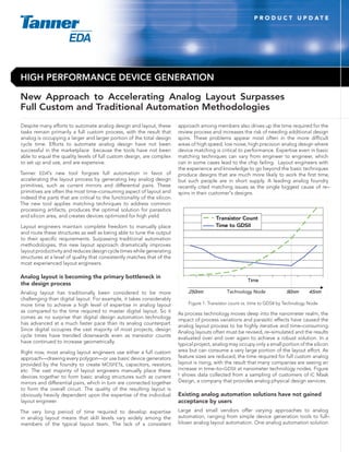
  • 1. P R O D U C T U P D AT E HIGH PERFORMANCE DEVICE GENERATION New Approach to Accelerating Analog Layout Surpasses Full Custom and Traditional Automation Methodologies Despite many efforts to automate analog design and layout, these approach among members also drives up the time required for the tasks remain primarily a full custom process, with the result that review process and increases the risk of needing additional design analog is occupying a larger and larger portion of the total design spins. These problems appear most often in the more difficult cycle time. Efforts to automate analog design have not been areas of high speed, low noise, high precision analog design where successful in the marketplace because the tools have not been device matching is critical to performance. Expertise even in basic able to equal the quality levels of full custom design, are complex matching techniques can vary from engineer to engineer, which to set up and use, and are expensive. can in some cases lead to the chip failing. Layout engineers with the experience and knowledge to go beyond the basic techniques Tanner EDA’s new tool forgoes full automation in favor of produce designs that are much more likely to work the first time, accelerating the layout process by generating key analog design but such people are in short supply. A leading analog foundry primitives, such as current mirrors and differential pairs. These recently cited matching issues as the single biggest cause of re– primitives are often the most time–consuming aspect of layout and spins in their customer’s designs. indeed the parts that are critical to the functionality of the silicon. The new tool applies matching techniques to address common processing artifacts, produces the optimal solution for parasitics and silicon area, and creates devices optimized for high yield. Layout engineers maintain complete freedom to manually place and route these structures as well as being able to tune the output to their specific requirements. Surpassing traditional automation methodologies, this new layout approach dramatically improves layout productivity and reduces design cycle times while generating structures at a level of quality that consistently matches that of the most experienced layout engineers. Analog layout is becoming the primary bottleneck in the design process Analog layout has traditionally been considered to be more challenging than digital layout. For example, it takes considerably more time to achieve a high level of expertise in analog layout Figure 1: Transistor count vs. time to GDSII by Technology Node as compared to the time required to master digital layout. So it As process technology moves deep into the nanometer realm, the comes as no surprise that digital design automation technology impact of process variations and parasitic effects have caused the has advanced at a much faster pace than its analog counterpart. analog layout process to be highly iterative and time–consuming. Since digital occupies the vast majority of most projects, design Analog layouts often must be revised, re–simulated and the results cycle times have trended downwards even as transistor counts evaluated over and over again to achieve a robust solution. In a have continued to increase geometrically. typical project, analog may occupy only a small portion of the silicon Right now, most analog layout engineers use either a full custom area but can consume a very large portion of the layout effort. As approach—drawing every polygon—or use basic device generators feature sizes are reduced, the time required for full custom analog provided by the foundry to create MOSFETs, capacitors, resistors, layout is rising, with the result that many companies are seeing an etc. The vast majority of layout engineers manually place these increase in time–to–GDSII at nanometer technology nodes. Figure devices together to form basic analog structures such as current 1 shows data collected from a sampling of customers of IC Mask mirrors and differential pairs, which in turn are connected together Design, a company that provides analog physical design services. to form the overall circuit. The quality of the resulting layout is obviously heavily dependent upon the expertise of the individual Existing analog automation solutions have not gained layout engineer. acceptance by users The very long period of time required to develop expertise Large and small vendors offer varying approaches to analog in analog layout means that skill levels vary widely among the automation, ranging from simple device generation tools to full– members of the typical layout team. The lack of a consistent blown analog layout automation. One analog automation solution
  • 2. focuses on providing advanced editing features for creating and editing parameterized cells to expedite the process of creating matched structures. Another tool builds on the parameterized cell approach by adding many additional parameters and technology independence. Both operate only at the device level, so they do not address the layout of circuits and structures, which is not only the most time–consuming part of the analog layout process, but also the portion that is most prone to poor quality and inconsistency. Large amounts of time are required to generate individual structures by hand and the quality of the resulting layout varies depending upon the skill of the individual engineer. Another analog layout solution attempts to completely automate the analog layout process. It provides a programming language that allows users to code their own physical cells and its placement engine generates the layout based on these cells. But the coding takes place at a high level that does not take into consideration the basic characteristics of the key building blocks and may not lay Figure 2: Generation of structures based on existing DRC rules them out with the correct considerations. Users often find that the resulting designs do not compare in quality to a manually created Retargeting the components to a new technology node simply layout. Yet another tool takes as input a set of design rules and requires the user to input the manufacturing rules for that then generates basic structures, which are also placed and routed. technology and regenerate the devices and primitives. So it is One weakness of this approach is that it applies global matching possible to very quickly move a design to a new technology node rules to the entire layout while skilled manual designers understand or to a different foundry. that a current mirror, for example, should not be laid out in the same way as a differential pair. One more obstacle to adoption is HiPer DevGen was designed to be implemented with little or no its list price, which is quoted at close to a million dollars for a single change to existing design flows. Unlike existing full automation license. tools, it works with unmodified schematics. It also uses as input netlists produced for schematic driven layout (SDL) and also accepts Tanner EDA’s HiPer DevGen (High Performance Device input directly from S-Edit, Tanner EDA’s schematic editor. HiPer Generator) accelerates analog layout by automatically DevGen builds upon Tanner EDA’s existing T-Cell architecture of generating common structures parameterized cells that exist within the company’s L-Edit layout editor. The generated cells are cached in the database for maximum As we’ve seen above, previous methods to try to automate the performance. HiPer DevGen automatically recognizes the building analog design process have been primarily based either at the cell blocks of the design and generates technology–aware building level or at the level of the complete design. A new approach is blocks. The layout engineer then connects the blocks together and based on accelerating analog layout by generating primitives that wires them to pins to complete the design. are used over and over again such as current mirrors, differential pairs and resistor dividers. This approach creates these building blocks based on an understanding of the functional requirements Quality equals that which can be achieved by best that are needed to produce a high–quality layout. Rather than analog layout engineers attempting to completely automate analog design, HiPer DevGen The HiPer DevGen generation engine is “silicon–aware” and accelerates the most time–consuming aspects of the layout produces devices that are optimized for high yield, including process to substantially reduce the amount of time required for double contacts and vias and support for design for manufacturing analog layout while improving quality and design consistency. (DFM ) rules, where applicable. The generation engine takes into account over 20 common processing artifacts and applies matching By automatically generating the layout of devices—including techniques so that these processing effects are reduced where MOS transistors and resistors as well as MOS current mirrors, MOS possible or are applied equally across all matched devices. These differential pairs, resistor dividers and other basic structures—this artifacts include, but are not limited to: new approach provides nearly the same degree of acceleration as full automation, but with higher quality. As well as automating the » Linear process gradients tedious, repetitive aspects of the design process, HiPer DevGen also eliminates the complex and often very expensive setup » Mask misalignment process that is required with current analog automation tools. » Implant shadowing HiPer DevGen automatically generates both devices and analog » Photolithographic invariance design primitives using only the manufacturing design rules for the specific technology node as its input. The tool itself understands » Current flow direction the technology and matching requirements and automatically » Mechanical stress, including shallow trench isolation (STI ) generates the basic building blocks of analog layout with these or length of diffusion (LOD ) requirements taken into account. Layout engineers have complete freedom to lay out and place and route these structures. HiPer » Antenna effect/Vt shift DevGen is provided with basic default values that meet the requirements of 90% of analog designs. For example, in a differential » Well proximity effect (WPE) pair it will always attempt to optimize the drain parasitics over the HiPer DevGen ensures a consistent and high quality approach to source parasitics. However in circuits such as down mixers, where the layout of complex analog structures across layout engineers, the source capacitance is more critical, the designer or layout design teams and engineering sites. The generation engine engineer can easily change these parameters, regenerate, simulate considers device and interconnect parasitics and silicon area, the design and converge on an optimal design approach. and produces the optimal solution based on design inputs,
  • 3. foundry manufacturing rules, and user matching requirements. Figure 4 shows a more complex current mirror, again with dummies, Matching, parasitic, and performance considerations are tuned but in this case there are three output currents. In this case they to specific analog structures such as the previously mentioned are being scaled by two, two, and four respectively. This structure differences between current mirrors and differential pairs. The would take considerably longer than the first example (Figure 1) generation engine understands the key parameters associated if done by hand and its complexity increases the possibility of an with each structure and generates the structures so that these error that could cause rework or quality problems. HiPer DevGen key requirements are met while maintaining a continual focus on also generated this device instantly, with only the manufacturing silicon quality, yield, silicon performance, and matching. rules provided as input. The generation engine also can be adjusted to ensure that its output fits the user’s specific matching, parasitic, and performance requirements. For example, HiPer DevGen offers the user the ability to prioritize parasitic performance over matching requirements or vice versa, and also gives precedence to key matching concerns over others within a circuit. For instance on large devices, where a mismatch due to linear gradients is recognized as being a priority, the generation of the structure can be weighted towards that, as opposed to a possible mismatch in drain or source area. Examples of how this approach works in practice Figure 5: Two finger differential pair. Figure 5 shows a simple two fingered differential pair with a guard ring. In this case, the drain capacitance is optimized on both devices and the gates are densely connected in metal in order to reduce gate resistance and lower parasitic channel noise. While this example consists of only two transistors with two fingers each, the care required to lay out the structure increases the layout time dramatically. In conjunction with the increased layout effort, the risk of laying it out incorrectly, such as by optimizing the drain, also increases and these errors are typically only spotted either in silicon or where design flows ensure stringent extraction and post–layout Figure 3: Example current mirror simulation of all circuits. With HiPer DevGen, it is possible to create this instantly and, if necessary, generate multiple variants, allowing An example of a current mirror is shown in Figure 3. While an circuit designers to simulate each solution and converge on an experienced layout engineer would probably spend only a short optimal solution for their design in the shortest period of time. time to create this structure, the possibility exists that he or she might make an error that could take hours or even days to resolve later in the design cycle. Worse still, such as error could produce a circuit that is LVS and DRC–clean by construction, but has a mismatch, resulting in the problem only being seen in silicon. HiPer DevGen instantly created the structure shown, with the added assurance that it meets all requirements of the targeted technology. Figure 6: Eight finger differential pair Figure 6 shows a more complex differential pair with two devices of eight fingers each as well as a guard ring, protection diodes, and dummy devices. In this case, the capacitance of the source also is being optimized. A device of this complexity would take considerably more time than the previous example to lay out by Figure 4: Complex current mirror with dummies hand. Manual layout would also present considerable risk of error.
  • 4. For example, moving one of these devices by a micron could A number of analog layout engineers were asked how long it would introduce a mismatch into the device. HiPer DevGen instantly take them to lay out this circuit, while obeying best layout practice generated this device while simultaneously providing perfect and applying common matching techniques. Their answers ranged matching between both devices. from two hours to two days with an average time of approximately five hours. The complexity of the design means that nearly every engineer would do it differently and these differences have the potential, at best, to lengthen the review process or, at worst, to create yield problems or indeed non–functioning silicon. On the other hand, using HiPer DevGen, a layout engineer instantaneously generated all of the individual structures in the circuit, significantly reducing the overall design effort. The layout engineer then manually floorplanned the circuit and completed the interconnect between devices. Each device or structure was created exactly the same to meet all requirements of the technology, correct by construction in terms of passing layout versus. schematic checks (LVS ), DRC clean and with guaranteed matching. Using this approach, let’s suppose that the designer changes a parameter, such as increasing the number of fingers or making the block shorter or wider to fit a different floor plan. Or maybe multiple configurations are required to address parasitics Figure 7: Schematic of example circuit with 17 functional devices identified during simulation. If the design were done by hand, alternate versions would probably take just as long as the first version to lay out, consuming additional hours or days. With HiPer DevGen, the layout engineer can simply change a parameter and regenerate the structures that make up the design, completing the modifications in a matter of minutes. This acceleration in the design process makes it possible to reduce design cycle time by designing multiple parallel paths to see which one is best for any given circuit. For example, you might evaluate the ability of several different design alternatives to simulate the effects of artifacts such as LOD/STI or WPE. Conclusion HiPer DevGen increases analog layout productivity by accelerating the generation of devices and common analog structures. All cells are generated at a consistently high level of quality. Silicon quality, yield, silicon performance, and matching are as good as the best full custom layout engineer could produce and well above current fully automated layout generation. Design standards are the same Figure 8: Layout of example circuit with 17 functional devices for different designers and different projects. Re–targeting to new technology nodes is effortless. Figures 7 & 8 show a complete circuit. The top row of four transistors (two fingers in each device) is made up of two current mirrors, the next row of four transistors (two fingers in each device) is made up of two differential pairs and the bottom row of three transistors is another current mirror, comprising five gates in total. While not shown in the schematic, approximately ten dummy devices would also be required in order to ensure matching, bringing the total device count from seventeen to twenty–seven. Find out how HiPer DevGen can accelerate your analog layout design. Contact us at AnalogLayout@tannereda.com to schedule your evaluation. About Tanner EDA Tanner EDA provides of a complete line of software solutions that catalyze innovation for the design, layout and verification of analog and mixed-signal (A/MS) integrated circuits (ICs). Corporate Headquarters Customers are creating breakthrough applications in areas such as power management, displays 825 South Myrtle Avenue and imaging, automotive, consumer electronics, life sciences, and RF devices. A low learning Monrovia, CA 91016-3424 USA curve, high interoperability, and a powerful user interface improve design team productivity and Tel: +1-626-471-9700 enable a low total cost of ownership (TCO). Capability and performance are matched by low Toll Free: 877-325-2223 support requirements and high support capability as well as an ecosystem of partners that bring Fax: +1-626-471-9800 Email: sales@tannereda.com advanced capabilities to A/MS designs. Web: www.TannerEDA.com Founded in 1988, Tanner EDA solutions deliver the right mixture of features, functionality and © 2010 Tanner Research. All rights reserved. usability. The company has shipped over 33,000 licenses of its software to more than 5,000 All other company and/or product names are the customers in 67 countries. property of their respective owners.