
![TPS62230, TPS62231, TPS62232, TPS62233, TPS62234
TPS62235, TPS62236, TPS62237, TPS62238, TPS62239
TPS622310, TPS622311, TPS622312, TPS622313, TPS622314
SLVS941C – APRIL 2009 – REVISED APRIL 2010 www.ti.com
These devices have limited built-in ESD protection. The leads should be shorted together or the device placed in conductive foam
during storage or handling to prevent electrostatic damage to the MOS gates.
ORDERING INFORMATION
(1) FREQUENCY PACKAGE PACKAGE
TA PART NUMBER OUTPUT VOLTAGE (2) ORDERING
[MHz] DESIGNATOR MARKING
TPS62230 2.5 V 3 DRY TPS62230DRY GV
TPS62231 1.8 V 3 DRY TPS62231DRY GW
TPS62232 1.2 V 3 DRY TPS62232DRY GX
TPS62239 1.0 V 3 DRY TPS62239DRY OP
TPS622311 1.1V 2 DRY TPS622311DRY PA
TPS62235 1.2V 2 DRY TPS62235DRY OQ
TPS622313 1.3 V 3 DRY TPS62213DRY QG
TPS622314 1.5 V 3 DRY TPS622314DRY QF
–40°C to 85°C TPS62236 1.85V 2 DRY TPS62236DRY OR
TPS622312 2.0 V 3 DRY TPS622312DRY QE
TPS62234 2.1 V 3 DRY TPS62234DRY OH
TPS62238 2.25 V 3 DRY TPS62238DRY ON
TPS622310 2.3 V 3 DRY TPS622310DRY OT
(3)
TPS6223-2.7 2.7 V 3 DRY
TPS6223-2.9 (3) 2.9 V 3 DRY
TPS62233 3.0 V 3 DRY TPS62233DRY OG
TPS62237 3.3V 2 DRY TPS62237DRY OS
(1) The DRY package is available in tape on reel. Add R suffix to order quantities of 3000 parts per reel, T suffix for 250 parts per reel.
(2) Contact TI for other fixed output voltage options
(3) Device status is product preview, contact TI for more details
ABSOLUTE MAXIMUM RATINGS
(1)
over operating free-air temperature range (unless otherwise noted)
VALUE UNIT
Voltage at VIN and SW Pin (2) –0.3 to 7 V
VI Voltage at EN, MODE Pin (2) –0.3 to VIN +0.3, ≤7 V
(2)
Voltage at FB Pin –0.3 to 3.6 V
Peak output current internally limited A
HBM Human body model 2
kV
ESD rating (3) CDM Charge device model 1
Machine model 200 V
Power dissipation Internally limited
TJ Maximum operating junction temperature –40 to 125 °C
Tstg Storage temperature range –65 to 150 °C
(1) Stresses beyond those listed under absolute maximum ratings may cause permanent damage to the device. These are stress ratings
only and functional operation of the device at these or any other conditions beyond those indicated under recommended operating
conditions is not implied. Exposure to absolute–maximum–rated conditions for extended periods may affect device reliability.
(2) All voltage values are with respect to network ground terminal.
(3) The human body model is a 100-pF capacitor discharged through a 1.5-kΩ resistor into each pin. The machine model is a 200-pF
capacitor discharged directly into each pin.
2 Submit Documentation Feedback Copyright © 2009–2010, Texas Instruments Incorporated](data:image/gif;base64,R0lGODlhAQABAIAAAAAAAP///yH5BAEAAAAALAAAAAABAAEAAAIBRAA7)
Recomendados
Mais conteúdo relacionado
Mais procurados
Mais procurados (20)
Destaque
Destaque (18)
Semelhante a Datasheet of TPS62230
Semelhante a Datasheet of TPS62230 (20)
Mais de Tsuyoshi Horigome
Mais de Tsuyoshi Horigome (20)
Último
Último (20)
Datasheet of TPS62230
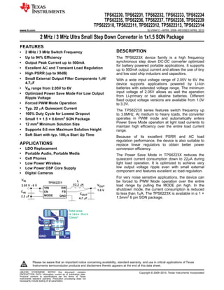
- 1. TPS62230, TPS62231, TPS62232, TPS62233, TPS62234 TPS62235, TPS62236, TPS62237, TPS62238, TPS62239 TPS622310, TPS622311, TPS622312, TPS622313, TPS622314 www.ti.com SLVS941C – APRIL 2009 – REVISED APRIL 2010 2 MHz / 3 MHz Ultra Small Step Down Converter in 1x1.5 SON Package 1FEATURES • 2 MHz / 3 MHz Switch Frequency DESCRIPTION • Up to 94% Efficiency The TPS6223X device family is a high frequency • Output Peak Current up to 500mA synchronous step down DC-DC converter optimized for battery powered portable applications. It supports • Excellent AC and Transient Load Regulation up to 500mA output current and allows the use of tiny • High PSRR (up to 90dB) and low cost chip inductors and capacitors. • Small External Output Filter Components 1mH/ With a wide input voltage range of 2.05V to 6V the 4.7mF device supports applications powered by Li-Ion • VIN range from 2.05V to 6V batteries with extended voltage range. The minimum • Optimized Power Save Mode For Low Output input voltage of 2.05V allows as well the operation from Li-primary or two alkaline batteries. Different Ripple Voltage fixed output voltage versions are available from 1.0V • Forced PWM Mode Operation to 3.3V. • Typ. 22 mA Quiescent Current The TPS6223X series features switch frequency up • 100% Duty Cycle for Lowest Dropout to 3.8MHz. At medium to heavy loads, the converter • Small 1 × 1.5 × 0.6mm3 SON Package operates in PWM mode and automatically enters Power Save Mode operation at light load currents to • 12 mm2 Minimum Solution Size maintain high efficiency over the entire load current • Supports 0.6 mm Maximum Solution Height range. • Soft Start with typ. 100ms Start Up Time Because of its excellent PSRR and AC load regulation performance, the device is also suitable to APPLICATIONS replace linear regulators to obtain better power • LDO Replacement conversion efficiency. • Portable Audio, Portable Media The Power Save Mode in TPS6223X reduces the • Cell Phones quiescent current consumption down to 22mA during • Low Power Wireless light load operation. It is optimized to achieve very • Low Power DSP Core Supply low output voltage ripple even with small external component and features excellent ac load regulation. • Digital Cameras For very noise sensitive applications, the device can VIN TPS62231 L be forced to PWM Mode operation over the entire 2.05 V - 6 V 1/2.2 mH VOUT load range by pulling the MODE pin high. In the VIN SW 1.8 V shutdown mode, the current consumption is reduced CIN EN FB COUT to less than 1mA. The TPS6223X is available in a 1 × 2.2 mF MODE GND 4.7 mF 1.5mm2 6 pin SON package. Total area L1 12mm² V IN C1 C2 GND V OUT 1 Please be aware that an important notice concerning availability, standard warranty, and use in critical applications of Texas Instruments semiconductor products and disclaimers thereto appears at the end of this data sheet. UNLESS OTHERWISE NOTED this document contains Copyright © 2009–2010, Texas Instruments Incorporated PRODUCTION DATA information current as of publication date. Products conform to specifications per the terms of Texas Instruments standard warranty. Production processing does not necessarily include testing of all parameters.
- 2. TPS62230, TPS62231, TPS62232, TPS62233, TPS62234 TPS62235, TPS62236, TPS62237, TPS62238, TPS62239 TPS622310, TPS622311, TPS622312, TPS622313, TPS622314 SLVS941C – APRIL 2009 – REVISED APRIL 2010 www.ti.com These devices have limited built-in ESD protection. The leads should be shorted together or the device placed in conductive foam during storage or handling to prevent electrostatic damage to the MOS gates. ORDERING INFORMATION (1) FREQUENCY PACKAGE PACKAGE TA PART NUMBER OUTPUT VOLTAGE (2) ORDERING [MHz] DESIGNATOR MARKING TPS62230 2.5 V 3 DRY TPS62230DRY GV TPS62231 1.8 V 3 DRY TPS62231DRY GW TPS62232 1.2 V 3 DRY TPS62232DRY GX TPS62239 1.0 V 3 DRY TPS62239DRY OP TPS622311 1.1V 2 DRY TPS622311DRY PA TPS62235 1.2V 2 DRY TPS62235DRY OQ TPS622313 1.3 V 3 DRY TPS62213DRY QG TPS622314 1.5 V 3 DRY TPS622314DRY QF –40°C to 85°C TPS62236 1.85V 2 DRY TPS62236DRY OR TPS622312 2.0 V 3 DRY TPS622312DRY QE TPS62234 2.1 V 3 DRY TPS62234DRY OH TPS62238 2.25 V 3 DRY TPS62238DRY ON TPS622310 2.3 V 3 DRY TPS622310DRY OT (3) TPS6223-2.7 2.7 V 3 DRY TPS6223-2.9 (3) 2.9 V 3 DRY TPS62233 3.0 V 3 DRY TPS62233DRY OG TPS62237 3.3V 2 DRY TPS62237DRY OS (1) The DRY package is available in tape on reel. Add R suffix to order quantities of 3000 parts per reel, T suffix for 250 parts per reel. (2) Contact TI for other fixed output voltage options (3) Device status is product preview, contact TI for more details ABSOLUTE MAXIMUM RATINGS (1) over operating free-air temperature range (unless otherwise noted) VALUE UNIT Voltage at VIN and SW Pin (2) –0.3 to 7 V VI Voltage at EN, MODE Pin (2) –0.3 to VIN +0.3, ≤7 V (2) Voltage at FB Pin –0.3 to 3.6 V Peak output current internally limited A HBM Human body model 2 kV ESD rating (3) CDM Charge device model 1 Machine model 200 V Power dissipation Internally limited TJ Maximum operating junction temperature –40 to 125 °C Tstg Storage temperature range –65 to 150 °C (1) Stresses beyond those listed under absolute maximum ratings may cause permanent damage to the device. These are stress ratings only and functional operation of the device at these or any other conditions beyond those indicated under recommended operating conditions is not implied. Exposure to absolute–maximum–rated conditions for extended periods may affect device reliability. (2) All voltage values are with respect to network ground terminal. (3) The human body model is a 100-pF capacitor discharged through a 1.5-kΩ resistor into each pin. The machine model is a 200-pF capacitor discharged directly into each pin. 2 Submit Documentation Feedback Copyright © 2009–2010, Texas Instruments Incorporated
- 3. TPS62230, TPS62231, TPS62232, TPS62233, TPS62234 TPS62235, TPS62236, TPS62237, TPS62238, TPS62239 TPS622310, TPS622311, TPS622312, TPS622313, TPS622314 www.ti.com SLVS941C – APRIL 2009 – REVISED APRIL 2010 DISSIPATION RATINGS (1) POWER RATING DERATING FACTOR PACKAGE RqJA FOR TA ≤ 25°C ABOVE TA = 25°C 1 × 1.5 SON 234°C/W (2) 420 mW 4.2 mW/°C (1) Maximum power dissipation is a function of TJ(max), qJA and TA. The maximum allowable power dissipation at any allowable ambient temperature is PD = [TJ(max) – TA] /qJA. (2) This thermal data is measured with high-K board (4 layers board according to JESD51-7 JEDEC standard). RECOMMENDED OPERATING CONDITIONS operating ambient temperature TA = –40 to 85°C (unless otherwise noted) (1) MIN NOM MAX UNIT (2) Supply voltage VIN 2.05 6 V Effective inductance 2.2 mH Effective capacitance 2.0 4.7 mF VOUT ≤ VIN -1 V (3) 500 mA maximum IOUT (4) 3.0 3.6 Recommended minimum (5) 350mA maximum IOUT 2.5 2.7 V supply voltage VOUT ≤ 1.8V 60 mA maximum output current (5) 2.05 Operating virtual junction temperature range, TJ –40 125 °C (1) In applications where high power dissipation and/or poor package thermal resistance is present, the maximum ambient temperature may have to be derated. Maximum ambient temperature (TA(max)) is dependent on the maximum operating junction temperature (TJ(max)), the maximum power dissipation of the device in the application (PD(max)), and the junction-to-ambient thermal resistance of the part/package in the application (qJA), as given by the following equation: TA(max) = TJ(max) – (qJA × PD(max)). (2) The minimum required supply voltage for startup is 2.05 V. The part is functional down to the falling UVL (Under Voltage Lockout) threshold. (3) For a voltage difference between minimum VIN and VOUT of ≥ 1 V (4) Typical value applies for TA = 25°C, maximum value applies for TA = 70°C with TJ ≤ 125°C, PCB layout needs to support proper thermal performance. (5) Typical value applies for TA = 25°C, maximum value applies for TA = 85°C with TJ ≤ 125°C, PCB layout needs to support proper thermal performance. Copyright © 2009–2010, Texas Instruments Incorporated Submit Documentation Feedback 3
- 4. TPS62230, TPS62231, TPS62232, TPS62233, TPS62234 TPS62235, TPS62236, TPS62237, TPS62238, TPS62239 TPS622310, TPS622311, TPS622312, TPS622313, TPS622314 SLVS941C – APRIL 2009 – REVISED APRIL 2010 www.ti.com ELECTRICAL CHARACTERISTICS VIN = 3.6V, VOUT = 1.8V, EN = VIN, MODE = GND, TA = –40°C to 85°C (1) typical values are at TA = 25°C (unless otherwise noted), CIN = 2.2mF, L = 2.2mH, COUT = 4.7mF, see parameter measurement information PARAMETER TEST CONDITIONS MIN TYP MAX UNIT SUPPLY (2) VIN Input voltage range 2.05 6 V IOUT = 0mA. PFM mode enabled (Mode = 0) 22 40 mA device not switching IOUT = 0mA. PFM mode enabled (Mode = 0) IQ Operating quiescent current 25 mA device switching, VIN = 3.6V, VOUT = 1.2V IOUT = 0 mA. Switching with no load (MODE/DATA = VIN), PWM operation, 3 mA VOUT = 1.8V, L = 2.2mH ISD Shutdown current EN = GND (3) 0.1 1 mA Falling 1.8 1.9 V UVLO Undervoltage lockout threshold Rising 1.9 2.05 V ENABLE, MODE THRESHOLD VIH TH Threshold for detecting high EN, MODE 2.05 V ≤ VIN ≤ 6V , rising edge 0.8 1 V VIL TH HYS Threshold for detecting low EN, MODE 2.05 V ≤ VIN ≤ 6V , falling edge 0.4 0.6 V IIN Input bias Current, EN, MODE EN, MODE = GND or VIN = 3.6V 0.01 0.5 mA POWER SWITCH High side MOSFET on-resistance 600 850 RDS(ON) VIN = 3.6V, TJmax = 85°C; RDS(ON) max value mΩ Low Side MOSFET on-resistance 350 480 Forward current limit MOSFET 690 850 1050 mA ILIMF high-side VIN = 3.6V, open loop Forward current limit MOSFET low side 550 840 1220 mA TSD Thermal shutdown Increasing junction temperature 150 °C Thermal shutdown hysteresis Decreasing junction temperature 20 °C CONTROLLER tONmin Minimum ON time VIN 3.6V, VOUT = 1.8V, Mode = high, IOUT = 0 mA 135 ns tOFFmin Minimum OFF time 40 ns OUTPUT VREF Internal Reference Voltage 0.70 V VIN = 3.6V, Mode = GND, device operating in PFM 0% Mode, IOUT = 0mA (4) Output voltage accuracy VIN = 3.6V, MODE = VIN, TA = 25°C –2.0% 2.0% VOUT IOUT = 0 mA TA = –40°C to 85°C –2.5% 2.5% DC output voltage load regulation PWM operation, Mode = VIN = 3.6V, VOUT = 1.8 V 0.001 %/mA DC output voltage line regulation IOUT = 0 mA, Mode = VIN, 2.05V ≤ VIN ≤ 6V 0 %/V Time from active EN to VOUT = 1.8V, VIN = 3.6V, tStart Start-up Time 100 ms 10Ω load (5) ILK_SW Leakage current into SW pin VIN = VOUT = VSW = 3.6 V, EN = GND 0.1 0.5 mA (1) In applications where high power dissipation and/or poor package thermal resistance is present, the maximum ambient temperature may have to be derated. Maximum ambient temperature (TA(max)) is dependent on the maximum operating junction temperature (TJ(max)), the maximum power dissipation of the device in the application (PD(max)), and the junction-to-ambient thermal resistance of the part/package in the application (qJA), as given by the following equation: TA(max) = TJ(max) – (qJA × PD(max)). (2) The minimum required supply voltage for startup is 2.05V. The part is functional down to the falling UVL (Under Voltage Lockout) threshold (3) Shutdown current into VIN pin, includes internal leakage (4) VIN = VO + 1.0 V (5) The internal resistor divider network is disconnected from FB pin. 4 Submit Documentation Feedback Copyright © 2009–2010, Texas Instruments Incorporated
- 5. TPS62230, TPS62231, TPS62232, TPS62233, TPS62234 TPS62235, TPS62236, TPS62237, TPS62238, TPS62239 TPS622310, TPS622311, TPS622312, TPS622313, TPS622314 www.ti.com SLVS941C – APRIL 2009 – REVISED APRIL 2010 DRY PACKAGE (TOP VIEW) MODE 1 6 FB SW 2 5 EN VIN 3 4 GND PIN FUNCTIONS PIN I/O DESCRIPTION NAME NO VIN 3 PWR VIN power supply pin. GND 4 PWR GND supply pin EN 5 IN This is the enable pin of the device. Pulling this pin to low forces the device into shutdown mode. Pulling this pin to high enables the device. This pin must be terminated. SW 2 OUT This is the switch pin and is connected to the internal MOSFET switches. Connect the inductor to this terminal FB 6 IN Feedback Pin for the internal regulation loop. Connect this pin directly to the output capacitor. MODE 1 IN MODE pin = high forces the device to operate in PWM mode. Mode = low enables the Power Save Mode with automatic transition from PFM (Pulse frequency mode) to PWM (pulse width modulation) mode. FUNCTIONAL BLOCK DIAGRAM VIN VREF Undervoltage Current Bandgap Lockout 0.70 V Limit Comparator Limit High Side MODE MODE PMOS Softstart VIN Gate Driver Min. On Time Control Anti SW EN FB Logic Shoot-Through Min. OFF Time VREF NMOS FB Limit Low Side Integrated Feed Back Error Thermal Comparator Zero/Negative Network Shutdown Current Limit Comparator EN GND Copyright © 2009–2010, Texas Instruments Incorporated Submit Documentation Feedback 5
- 6. TPS62230, TPS62231, TPS62232, TPS62233, TPS62234 TPS62235, TPS62236, TPS62237, TPS62238, TPS62239 TPS622310, TPS622311, TPS622312, TPS622313, TPS622314 SLVS941C – APRIL 2009 – REVISED APRIL 2010 www.ti.com PARAMETER MEASUREMENT INFORMATION TPS6223X L = 1/2.2 mH VIN = 2.05 V to 6 V VOUT VIN SW CIN EN FB COUT 2.2 mF MODE GND 4.7 mF CIN: Murata GRM155R60J225ME15D 2.2 mF 0402 size COUT: Murata GRM188R60J475ME 4.7 mF 0603 size, VOUT >= 1.8 V COUT: Taiyo Yuden AMK105BJ475MV 4.7 mF 0402 size, VOUT = 1.2 V l: Murata LQM2HPN1R0MJ0 1 mH, LQM2HPN2R2MJ0 2.2 mH, 3 size 2.5x2.0x1.2mm TYPICAL CHARACTERISTICS Table of Graphs FIGURE h Efficiency vs Load current 1, 2, 3, 4, 5, 6, 7 h Efficiency vs Output Current 8, 9, 10, 11 12, 13, 14, 15, VO Output voltage vs Output current 16, 17 18, 19, 20, 21, Switching frequency vs Output current 22, 23, 24, 25, 26, 27 IQ Quiescent current vs Ambient temperature 28 ISD Shutdown current vs Ambient temperature 29 PMOS Static drain-source on-state resistance vs Supply voltage and ambient temperature 30 rDS(ON) NMOS Static drain-source on-state resistance vs Supply voltage and ambient temperature 31 PSRR Power supply rejection ratio vs Frequency 32 Typical operation 33, 34, 35 PFM 36 Line transient response PWM 37 Mode transition PFM / forced PWM 38 AC - load regulation performance 39, 40, 41 Load transient response 42, 43, 44, 45 Start-up 46, 47 Spurious Output Noise, 12R Load 48 Spurious Output Noise, 100R Load 49 6 Submit Documentation Feedback Copyright © 2009–2010, Texas Instruments Incorporated
- 7. TPS62230, TPS62231, TPS62232, TPS62233, TPS62234 TPS62235, TPS62236, TPS62237, TPS62238, TPS62239 TPS622310, TPS622311, TPS622312, TPS622313, TPS622314 www.ti.com SLVS941C – APRIL 2009 – REVISED APRIL 2010 TYPICAL CHARACTERISTICS (continued) 100 100 VIN = 3.6 V VIN = 2.9 V 90 90 VIN = 3.6 V 80 80 VIN = 4.2 V VIN = 2.9 V 70 70 VIN = 4.2 V VIN = 5 V Efficiency -% Efficiency -% 60 60 VIN = 5 V 50 50 40 40 30 30 MODE = GND, VOUT = 2.5V, MODE = VIN, 20 20 L = 2.2 mH (LQM2HPN2R2MJ0) VOUT = 2.5 V, 10 COUT = 4.7 mF 10 L = 2.2 mH (LQM2HPN2R2MJ0) COUT = 4.7 mF 0 0 0.1 1 10 100 1000 1 10 100 1000 IO - Output Current - mA IO - Output Current - mA Figure 1. Efficiency PFM/PWM Mode 2.5V Output Voltage Figure 2. Efficiency Forced PWM Mode 2.5V Output Voltage 100 100 VIN = 2.3 V 90 90 VIN = 2.3 V 80 VIN = 2.7 V 80 VIN = 2.7 V VIN = 3.3 V 70 70 VIN = 3.6 V VIN = 3.3 V Efficiency -% Efficiency -% 60 60 VIN = 4.2 V VIN = 3.6 V 50 50 VIN = 5 V VIN = 4.2 V 40 40 VIN = 5 V 30 30 MODE = GND, MODE = VIN, 20 VOUT = 1.8 V, 20 VOUT = 1.8 V, L = 2.2 mH (MIPSA25202R2), 10 COUT = 4.7 mF 10 L = 2.2 mH (MIPSA25202R2), COUT = 4.7 mF 0 0 0.1 1 10 100 1000 1 10 100 1000 IO - Output Current - mA IO - Output Current - mA Figure 3. Efficiency PFM/PWM MODE 1.8V Output Voltage Figure 4. Efficiency Forced PWM Mode 1.8V Output voltage Copyright © 2009–2010, Texas Instruments Incorporated Submit Documentation Feedback 7
- 8. TPS62230, TPS62231, TPS62232, TPS62233, TPS62234 TPS62235, TPS62236, TPS62237, TPS62238, TPS62239 TPS622310, TPS622311, TPS622312, TPS622313, TPS622314 SLVS941C – APRIL 2009 – REVISED APRIL 2010 www.ti.com TYPICAL CHARACTERISTICS (continued) 100 100 90 VIN = 2.3 V 90 80 80 VIN = 2.3 V 70 VIN = 2.7 V 70 VIN = 2.7 V VIN = 3.6 V Efficiency -% Efficiency -% 60 60 VIN = 3.6 V 50 VIN = 4.2 V VIN = 4.2 V 50 40 VIN = 5 V 40 VIN = 5 V 30 30 MODE = GND, MODE = VIN, 20 VOUT = 1.2 V, 20 VOUT = 1.2 V, L = 2.2 mH MIPSZ2012 2R2 (2012 size), 10 COUT = 4.7 mF 10 L = 2.2 mH MIPSZ2012 2R2 (2012 size), COUT = 4.7 mF 0 0 0.1 1 10 100 1000 1 10 100 1000 IO - Output Current - mA IO - Output Current - mA Figure 5. Efficiency PFM/PWM Mode 1.2V Output voltage Figure 6. Efficiency Forced PWM Mode 1.2V Output Voltage 90 100 VIN = 3.6 V 90 85 80 VIN = 5 V VIN = 4.2 V 80 MIPSA25202R2 L = 2.2 mH MIPSD1R0 70 (2.5x2x1.2mm3) L = 1 mH 0805 75 Efficiency -% Efficiency - % (2x1.25x1mm3) LQM2HPN1R0MJ0 60 L = 1 mH MIPSZ2012D2R2 (2.5x2x1.2mm3) 70 50 L = 2.2 mH 0805 (2x1.25x1mm3) 40 65 LQM21PN2R2 L = 2.2 mH 0805 MODE = GND, 30 TPS62233 60 (2x1.25x0.55mm3) CIN = 2.2 mF (0402), MODE = GND, COUT = 4.7 mF (0402), 20 VOUT = 3 V, 55 VOUT = 1.8 V, L = 1 mH, 10 COUT = 4.7 mF VIN = 3.6 V 50 0 0.1 1 10 100 1000 0.1 1 10 100 1000 IO - Output Current - mA IO - Output Current - mA Figure 7. Comparison Efficiency vs Inductor Value and Size Figure 8. Comparison Efficiency vs IOUT – TPS62233 8 Submit Documentation Feedback Copyright © 2009–2010, Texas Instruments Incorporated
- 9. TPS62230, TPS62231, TPS62232, TPS62233, TPS62234 TPS62235, TPS62236, TPS62237, TPS62238, TPS62239 TPS622310, TPS622311, TPS622312, TPS622313, TPS622314 www.ti.com SLVS941C – APRIL 2009 – REVISED APRIL 2010 TYPICAL CHARACTERISTICS (continued) 90 100 VIN = 3.3 V VIN = 3.3 V 90 80 VIN = 3.6 V 80 VIN = 3.6 V 70 VIN = 4.2 V Efficiency - % Efficiency - % VIN = 4.2 V 70 60 60 50 50 40 40 VOUT = 1.2 V PFM, TPS62236 VOUT = 1.85 V PFM MODE = GND 30 30 0.1 1 10 100 1000 0.1 1 10 100 1000 IO - Output Current - mA IO - Output Current - mA Figure 9. Comparison Efficiency vs IOUT – TPS62235 Figure 10. Comparison Efficiency vs IOUT – TPS62236 90 2.575 VIN = 3.3 V MODE = VIN, VOUT = 2.5 V, 80 2.55 L = 1 mH, VIN = 3.6 V COUT = 4.7 mF, VO - Output Voltage (DC) - V TA = 25°C VIN = 3.3 V 70 VIN = 4.2 V 2.525 Efficiency - % VIN = 3.6 V 60 2.5 VIN = 4.2 V 50 2.475 VIN = 5 V 40 2.45 TPS622311 VOUT = 1.1 V PFM 30 2.425 0.1 1 10 100 1000 0.1 1 10 100 1000 IO - Output Current - mA IO - Output Current - mA Figure 11. Comparison Efficiency vs IOUT – TPS622311 Figure 12. 2.5V Output Voltage Accuracy forced PWM Mode Copyright © 2009–2010, Texas Instruments Incorporated Submit Documentation Feedback 9
- 10. TPS62230, TPS62231, TPS62232, TPS62233, TPS62234 TPS62235, TPS62236, TPS62237, TPS62238, TPS62239 TPS622310, TPS622311, TPS622312, TPS622313, TPS622314 SLVS941C – APRIL 2009 – REVISED APRIL 2010 www.ti.com TYPICAL CHARACTERISTICS (continued) 2.575 1.854 MODE = GND, MODE = GND, VOUT = 2.5 V, VOUT = 1.8 V, L = 1 mH, 2.55 1.836 L = 2.2 mH, COUT = 4.7 mF, COUT = 4.7 mF, VO - Output Voltage (DC) - V VO - Output Voltage (DC) - V TA = 25°C TA = 25°C 2.525 VIN = 4.2 V VIN = 5 V 1.818 VIN = 3.6 V VIN = 3.3 V 2.5 VIN = 3.3 V 1.8 VIN = 3.6 V VIN = 4.2 V 2.475 1.782 VIN = 5 V 2.45 1.764 2.425 1.746 0.1 1 10 100 1000 0.01 0.1 1 10 100 1000 IO - Output Current - mA IO - Output Current - mA Figure 13. 2.5V Output Voltage Accuracy PFM/PWM Mode Figure 14. 1.8V Output Voltage Accuracy PFM/PWM Mode 1.854 1.236 MODE = VIN, MODE = VIN, VOUT = 1.8 V, VOUT = 1.2 V, 1.836 L = 1 mH, 1.224 L = 2.2 mH, COUT = 4.7 mF, COUT = 4.7 mF, VO - Output Voltage (DC) - V VO - Output Voltage (DC) - V TA = 25°C TA = 25°C VIN = 3.3 V VIN = 3.3 V 1.818 VIN = 3.6 V 1.212 VIN = 3.6 V 1.8 1.2 VIN = 5 V VIN = 4.2 V 1.782 VIN = 4.2 V 1.188 VIN = 5 V 1.764 1.176 1.746 1.164 0.1 1 10 100 1000 0.1 1 10 100 1000 IO - Output Current - mA IO - Output Current - mA Figure 15. 1.8V Output Voltage Accuracy Forced PWM MODE Figure 16. 1.2V Output Voltage Accuracy Forced PWM MODE 10 Submit Documentation Feedback Copyright © 2009–2010, Texas Instruments Incorporated
- 11. TPS62230, TPS62231, TPS62232, TPS62233, TPS62234 TPS62235, TPS62236, TPS62237, TPS62238, TPS62239 TPS622310, TPS622311, TPS622312, TPS622313, TPS622314 www.ti.com SLVS941C – APRIL 2009 – REVISED APRIL 2010 TYPICAL CHARACTERISTICS (continued) 1.236 4000 MODE = GND, VOUT = 1.2 V, 3500 VIN = 5 V 1.224 L = 2.2 mH, COUT = 4.7 mF, VIN = 4.2 V VO - Output Voltage (DC) - V TA = 25°C 3000 VIN = 3.3 V VIN = 3.6 V 1.212 f - Frequency - kHz VIN = 3.3 V 2500 VIN = 3.6 V 1.2 2000 VIN = 4.2 V 1500 1.188 VIN = 5 V MODE = GND, 1000 VIN = 2.7 V VOUT = 1.8 V, 1.176 L = 2.2 mH, 500 VIN = 2.3 V COUT = 4.7 mF, TA = 25°C 1.164 0 0.01 0.1 1 10 100 1000 0 100 200 300 400 500 IO - Output Current - mA IO - Output Current - mA Figure 17. 1.2V Output Voltage Accuracy PFM/PWM MODE Figure 18. Switching Frequency vs Output Current, 1.8V Output Voltage MODE = GND 4000 4000 VIN = 5 V VIN = 5 V 3500 VIN = 4.2 V 3500 VIN = 4.2 V VIN = 3.6 V VIN = 3.6 V 3000 3000 VIN = 3.3 V VIN = 3.3 V f - Frequency - kHz f - Frequency - kHz 2500 2500 2000 2000 1500 1500 MODE = GND, MODE = VIN, 1000 VOUT = 1.8 V, 1000 VIN = 2.7 V VIN = 2.7 V VOUT = 1.8 V, L = 1 mH, VIN = 2.3 V VIN = 2.3 V L = 2.2 mH, 500 COUT = 4.7 mF, 500 COUT = 4.7 mF, TA = 25°C TA = 25°C 0 0 0 100 200 300 400 500 0 100 200 300 400 500 IO - Output Current - mA IO - Output Current - mA Figure 19. Switching Frequency vs Output Current, 1.8V Output Figure 20. Switching Frequency vs Output Current, 1.8V Output Voltage MODE = GND Voltage MODE = VIN Copyright © 2009–2010, Texas Instruments Incorporated Submit Documentation Feedback 11
- 12. TPS62230, TPS62231, TPS62232, TPS62233, TPS62234 TPS62235, TPS62236, TPS62237, TPS62238, TPS62239 TPS622310, TPS622311, TPS622312, TPS622313, TPS622314 SLVS941C – APRIL 2009 – REVISED APRIL 2010 www.ti.com TYPICAL CHARACTERISTICS (continued) 4000 4000 MODE = GND, VIN = 5 V MODE = VIN, VOUT = 2.5 V, VIN = 4.2 V VOUT = 2.5 V, 3500 VIN = 5 V 3500 L = 2.2 mH, VIN = 3.6 V L = 2.2 mH, VIN = 4.2 V COUT = 4.7 mF, COUT = 4.7 mF, 3000 3000 VIN = 3.3 V TA = 25°C TA = 25°C f - Frequency - kHz f - Frequency - kHz 2500 2500 VIN = 3.6 V 2000 2000 VIN = 3.3 V 1500 1500 1000 1000 500 VIN = 3 V 500 VIN = 3 V 0 0 0 100 200 300 400 500 0 100 200 300 400 500 IO - Output Current - mA IO - Output Current - mA Figure 21. Switching Frequency vs Output Current, 2.5V Output Figure 22. Switching Frequency vs Output Current, 2.5V Output Voltage MODE = GND Voltage MODE = VIN 3500 3000 VIN = 5 V VIN = 5 V 3000 VIN = 4.2 V 2500 VIN = 4.2 V VIN = 3.3 V VIN = 3.6 V 2500 VIN = 3.6 V VIN = 3.3 V f - Frequency - kHz f - Frequency - kHz 2000 VIN = 2.7 V 2000 1500 1500 VIN = 2.3 V 1000 VIN = 2 V VIN = 2.7 V 1000 VIN = 2.3 V MODE = GND, VOUT = 1.2 V, MODE = VIN, VIN = 2 V VOUT = 1.2 V, L = 2.2 mH, 500 L = 2.2 mH, 500 COUT = 4.7 mF, TA = 25°C COUT = 4.7 mF, TA = 25°C 0 0 0 100 200 300 400 500 0 100 200 300 400 500 IO - Output Current - mA IO - Output Current - mA Figure 23. Switching Frequency vs Output Current, 1.2V Output Figure 24. Switching Frequency vs Output Current, 1.2V Output Voltage MODE = GND Voltage MODE = VIN 12 Submit Documentation Feedback Copyright © 2009–2010, Texas Instruments Incorporated
- 13. TPS62230, TPS62231, TPS62232, TPS62233, TPS62234 TPS62235, TPS62236, TPS62237, TPS62238, TPS62239 TPS622310, TPS622311, TPS622312, TPS622313, TPS622314 www.ti.com SLVS941C – APRIL 2009 – REVISED APRIL 2010 TYPICAL CHARACTERISTICS (continued) 2500 3000 VIN = 5 V VIN = 4.2 V VIN = 5 V VIN = 3.6 V 2500 2000 VIN = 4.2 V f - Frequency - KHz f - Frequency - KHz 2000 1500 VIN = 2.3 V VIN = 2.7 V VIN = 3.3 V 1500 VIN = 3.3 V 1000 1000 VIN = 3.6 V TPS62235 MODE = GND, TPS62236 VIN = 2.7 V MODE = GND, 500 VOUT = 1.2 V, 500 VIN = 2.3 V VOUT = 1.85 V, L = 2.2 mH, L = 2.2 mH, COUT = 4.7 mF COUT = 4.7 mF 0 0 0 0.05 0.10 0.15 0.20 0.25 0.30 0.35 0.40 0.45 0.50 0 0.05 0.1 0.15 0.2 0.25 0.3 0.35 0.4 0.45 IO - Output Current - A IO - Output Current - A Figure 25. Switching Frequency vs Output Current, 1.2V Output Figure 26. Switching Frequency vs Output Current, 1.85V Voltage MODE = PFM – TPS62235 Output Voltage MODE = PFM –TPS62236 3000 35 TA = 85°C 2500 TA = 60°C TA = 25°C 30 VIN = 5 V IQ - Quiescent Current - mA VIN = 4.2 V f - Frequency - KHz 2000 25 1500 VIN = 2.7 V VIN = 3.3 V 20 VIN = 2.3 V TA = -40°C 1000 TPS622311 MODE = GND, VOUT = 1.1 V, 15 500 L = 2.2 mH, COUT = 4.7 mF 0 0 0.05 0.10 0.15 0.20 0.25 0.30 0.35 0.40 0.45 0.50 10 2 2.5 3 3.5 4 4.5 5 5.5 6 IO - Output Current - A VIN - Input Voltage - V Figure 27. Switching Frequency vs Output Current, 1.1V Output Figure 28. Quiescent Current IQ vs Ambient Temperature TA Voltage MODE = PFM – TPS622311 Copyright © 2009–2010, Texas Instruments Incorporated Submit Documentation Feedback 13
- 14. TPS62230, TPS62231, TPS62232, TPS62233, TPS62234 TPS62235, TPS62236, TPS62237, TPS62238, TPS62239 TPS622310, TPS622311, TPS622312, TPS622313, TPS622314 SLVS941C – APRIL 2009 – REVISED APRIL 2010 www.ti.com TYPICAL CHARACTERISTICS (continued) 0.2 rDS(ON) - Static Drain-Source On-State Resistance - W 2 PMOS 0.18 TA = 85°C 1.8 TA = 85°C 0.16 1.6 TA = 60°C ISD - Shutdown Current - mA 0.14 1.4 TA = 25°C 0.12 1.2 TA = -40°C 0.1 1 0.08 TA = -40°C 0.8 TA = 60°C TA = 25°C 0.06 0.6 0.04 0.4 0.02 0.2 0 0 2 2.5 3 3.5 4 4.5 5 5.5 6 2 2.5 3 3.5 4 4.5 5 5.5 6 VIN - Input Voltage - V VIN - Input Voltage - V Figure 29. Shutdown Current ISD vs Ambient Temperature TA Figure 30. PMOS RDSON vs Supply Voltage VIN and Ambient Temperature TA 100 rDS(ON) - Static Drain-Source On-State Resistance - W 0.7 NMOS IOUT = 50 mA, 90 PSRR - Power Supply Rejection Ratio - dB TA = 85°C MODE = 0, 0.6 forced PWM TA = 60°C 80 0.5 TA = 25°C 70 TA = -40°C 60 IOUT = 50 mA, 0.4 MODE = 1, 50 PFM/PWM IOUT = 150 mA, 0.3 40 PWM Mode 30 VIN = 3.6 V, 0.2 VOUT = 1.8 V, 20 CIN = 2.2 mF, 0.1 10 COUT = 4.7 mF, L = 2.2 mH 0 0 10 100 1k 10k 100k 1M 2 2.5 3 3.5 4 4.5 5 5.5 6 f - Frequency - kHz VIN - Input Voltage - V Figure 31. NMOS RDSON vs Supply Voltage VIN and Ambient Figure 32. TPS62231 1.8V PSRR Temperature TA 14 Submit Documentation Feedback Copyright © 2009–2010, Texas Instruments Incorporated
- 15. TPS62230, TPS62231, TPS62232, TPS62233, TPS62234 TPS62235, TPS62236, TPS62237, TPS62238, TPS62239 TPS622310, TPS622311, TPS622312, TPS622313, TPS622314 www.ti.com SLVS941C – APRIL 2009 – REVISED APRIL 2010 TYPICAL CHARACTERISTICS (continued) SW VIN = 3.6 V 2 V/div VOUT = 2.5V COUT = 4.7 mF 20 mV/div L = 2.2 mH VIN = 3.6V MODE = GND COUT = 4.7 mF SW IOUT = 10 mA VOUT = 2.5V 2 V/div 20 mV/Div L = 1 mH MODE = GND IOUT = 10 mA IL IL 200 mA/Div 200 mA/div t - Time - 1 ms/div t - Time - 1 ms/div Figure 33. PFM Mode Operation IOUT = 10mA Figure 34. PFM Mode Operation IOUT = 10mA MODE = VIN VIN = 3.6 V VOUT = 2.5 V IOUT = 10 mA COUT = 4.7 mF L = 1 mH VIN = 3.6 V to 4.2 V 20 mV/div 200 mV/div SW 2 V/div IL 200 mA/div VOUT = 1.8 V COUT = 4.7 mF 20 mV/div L = 2.2 mH MODE = GND IOUT = 50 mA t - Time - 500 ns/div t - Time - 10 ms/div Figure 35. Forced PWM Mode Operation IOUT = 10mA Figure 36. Line Transient Response PFM Mode Copyright © 2009–2010, Texas Instruments Incorporated Submit Documentation Feedback 15
- 16. TPS62230, TPS62231, TPS62232, TPS62233, TPS62234 TPS62235, TPS62236, TPS62237, TPS62238, TPS62239 TPS622310, TPS622311, TPS622312, TPS622313, TPS622314 SLVS941C – APRIL 2009 – REVISED APRIL 2010 www.ti.com TYPICAL CHARACTERISTICS (continued) VIN = 3.6 V to 4.2 V MODE: 0 V to 3.6 V Forced PWM 2 V/div Mode Operation 200 mV/div PFM Mode Operation VSW 2 V/div VIN = 3.6 V, COUT = 4.7 mF ICOIL L = 1 mH 200 mA/div IOUT = 10 mA VOUT = 1.8 V COUT = 4.7 mF 20 mV/div L = 2.2 mH MODE = VIN VOUT = 1.8 V IOUT = 50 mA 20 mV/div t - Time - 100 ms/div t - Time - 1 ms/div Figure 37. Line Transient Response PWM Mode Figure 38. Mode Transition PFM / Forced PWM Mode VIN = 3.6 V VOUT = 2.5 V VOUT = 2.5 V COUT = 4.7 mF 50 mV/div 50 mV/div L = 2.2 mH MODE = GND VIN = 3.6 V IOUT = 5 mA to 200 mA IOUT = 5mA to 200mA COUT = 4.7 mF sinusoidal sinusoidal L = 2.2 mH 100 mA/div 100mA/Div MODE = VIN IL IL 200 mA/div 200 mA/div t - Time - 5 ms/div t - Time - 5 ms/div Figure 39. AC – Load Regulation Performance 2.5V VOUT PFM Figure 40. AC – Load Regulation Performance 2.5V VOUT PWM Mode Mode 16 Submit Documentation Feedback Copyright © 2009–2010, Texas Instruments Incorporated