SlideShare uma empresa Scribd logo
1 de 5
Baixar para ler offline
Frequency Peaking Compensation
                                                                                              of the GX414 and GX424

by J. Ian Ridpath, Senior Applications Engineer, Video/Broadcast Products
                                                                                                                             APPLICATION NOTE

INTRODUCTION

In video switching applications, the crosspoint switch must                     The transfer function of this network is:
meet several critical specifications which include differential
                                                                                                                                   1
phase, differential gain and frequency response flatness.                                                   Vo                    LC       .......1
The GX4 family of crosspoint switches exceed broadcast                                            Ts =               =
requirements for the above specifications. For wide band-                                                   Vi           s2 + s    R   +    1
                                                                                                                                   L       LC
width and high bit rate data applications, the frequency/
                                                                                This transfer function has a pair of complex conjugate poles
flatness performance of these devices can be easily ex-
                                                                                with
tended using information in this application note. Information                                               1
                                                                                                   fo =                       ....... 2
presented gives the system designer two methods of fre-                                                  2     LC
quency compensating a system using the GX414 and GX424
                                                                                                                 1            L
Video Crosspoint Switches.                                                             and        Q =                                           ....... 3
                                                                                                                 R            C
The first method uses a small value series resistor placed in
the output of each device. The second method utilises the                       The frequency response peaks when Q >1/√2 at a frequency
frequency roll-off characteristics of the external video buffer                 equal to fo, but it is maximally flat when Q = 1/√2.
amplifier.
                                                                                In the above equations, the capacitance C, represents the
CHARACTERISTICS OF THE GX414 AND GX424                                          load capacitor external to the device. With any value of C, a
                                                                                value of R can be found which will make Q = 1/√2, thus
The GX414 and GX424 are bipolar video crosspoint switches                       flattening the response. Practically, this can be accomplished
configured as shown in Figure 1. Each analog switch has an                      by placing an external resistor in series with the output of the
emitter follower input, some level shifting and clamping                        device.
circuits and an emitter follower output. The four switch outputs
are tied together and brought out to one common pin. At                         In video routing or matrix switching applications, the load
frequencies above 1 MHz, the emitter follower switches nat-                     capacitance on the output bus is determined by how many
urally exhibit frequency response peaking.                                      devices are connected to the bus. A typical example as
                                                                                shown in Figure 3, uses five GX414s or five GX424s wired as
                                                             +Vcc               a 20 x 1 matrix.
                            CS
                                                                                                     IN 1
                                                                                                                         1             TO OUTPUT
                                                                                                                                       BUFFER


   IN
                                                             OUT                                                         2


                                                                                                                                       5 - GX414's
                                              CS    #2                                                                   3
         CS                                3 mA     #3                                                                                 CL = 4 x 15pF
                                                    #4                                                                                     = 60pF
                                                                                                                         4

                                                             -VEE

                                                                                                                         5
    Fig.1     Enabled Crosspoint Equivalent Circuit                                                 IN 20

The output impedance is roughly modelled as shown in Fig.                                            Fig.3           20 x 1 Matrix
                                          L
                                 R                 VO
                                                                                For any single selected crosspoint, four of the devices will be
                   +             44 Ω   180 nH
                                                                                disabled and one will be enabled (selected). The output
                       Vi
                                                         CLOAD
                                                                                capacitance of a disabled device is approximately 15 pF
                                                                                resulting in the total load capacitance seen by the selected
                                                                                device as approximately 60 pF. Assuming stray capacitance
                                                                                adds a further 5 pF to the system output, the total external

               Fig.2         Output Impedance Model


                                                                       510 - 39 - 00
Method 1. Adding Series Resistance to the Output

  Using equation 3), the value of R which will cause Q to equal                                  Precise modelling has been done yielding far more accurate
  1/√2 will be;                                                                                  results. The effect on the frequency response of any seriescom-
         R = ( √2 ) . √180 nH                                                                    pensating resistor can be computer simulated using these
                              ohms
                     √65pF                                                                       models. Figure 6 is an engineer-generated model of the
         which yields; R = 74.4 ohms                                                             GX414 or GX424 device. This model has been simulated
                                                                                                 using 'PSpice' (software by MicroSim Corporation) and com-
  Since the equivalent series output resistance of the device is                                 pared to measured results. A PSpice NETLIST is available on
  44 Ω (as shown in Figure 2), an additional 30.4 Ω must be                                      floppy disk from Gennum for assisting the systems engineer
  added in series with the output in order to make the total                                     and designer. The input and output impedance parameters
  resistance equal to 74.4 Ω. Figure 4 shows the frequency                                       are specified for frequencies up to 70 or 80 MHz and will
  response of the above set-up along with the uncompensated                                      produce accurate frequency response results for load ca-
  response. For this graph, a 33 Ω resistor was used and a 60                                    pacitances between 10 pF and 100 pF.
  pF load capacitor simulated the additional disabled devices.
                                                                                            IN   100                                   12          70n    12                             12       76n   OUT
                                                                                                                                                                   12
                2.5
                                                                                                                              50p
                2.0                                                                                       0.4 p                                                                           100
                                                                                                                                            100 50p
                                                               RS = 0 Ω                                       2K                                          2.5p
                                                                                                                              V1                                                  V2
                1.5                 CL = 60 pF                                                   1.5 p                                +            20p
                                                                                                                                                                                         +        50p
                                                                                                                                                                            21p                         14p
                1.0                                                                                       125          0.1p               V1
                                                                                                                                                           40     100
                                                                                                 2.2 p                                                                                   0.998 x V2     20
                0.5                                                                                              1.74 M        2K                                                 2.5p
   GAIN (dB)


                  0

                -0.5
                                                             R = 33Ω
                -1.0
                                                              S                                      Fig. 6        Engineer-generated Model of GX414 or GX424
                -1.5
                                                                                                 Figure 7 is an approximate model of a disabled crosspoint
                -2.0
                                                                                                 switch showing some of the circuit potentials and more
                -2.5                                                                             importantly, the various capacitances associated with a disa-
                       0                                10                        100
                                                                                                 bled switch.
                                                 FREQUENCY (MHz)

                  Fig. 4            Frequency and Uncompensated Responses
                                                                                                                 +8

  With the same 33 Ω resistor in the circuit, the load capacitors
                                                                                                                                                                        600 Ω
  were changed to 47 pF and 27 pF in order to see their effects
  on the frequency response. The 47pF capacitor closely                                                         V IN
                                                                                                                                                                        +
                                                                                                                                                          0.65 V
  simulates a 16 x 1 crosspoint circuit while the 27 pF approxi-
                                                                                                                               0.7pF           0.7pF     0.7pF
  mates a 10 x 1 situation. Figure 5 shows the results of these
  changes.                                                                                                                                                         0.7pF
                                                                                                                              1.5pF
                                                                                                                                               1.2K      2pF                             V OUT
               2.5
                                                                                                                                               +                 16pF
               2.0                                                                                                                             1.3 V
                                                                                                                                                                                    12pF
               1.5
                                                                                                                                                                                              ´
               1.0                      RS = 33 Ω
                                                                 27 pF
GAIN (dB)


               0.5
                                                                                                         Fig. 7           Disabled Crosspoint Equivalent Circuit
                 0
                                                                          47 pF
                                                                                                 The input capacitance of a disabled switch varies with the DC
               -0.5                                                                              bias voltage from 2.1 pF at -1 volt to 2.5 pF at +1.5 volts.
               -1.0                                                                              Futhermore, there is a slight change in CIN between the
                                                                                                 disabled state ( 2.2 pF at 0 volts bias ) and enabled state ( 2.0
               -1.5
                                                                                                 pF at 0 volts bias ). The slight variations would only be
               -2.0
                                                                                                 significant if the input driver source impedance is high. The
               -2.5                                                                              output capacitance of the disabled chip is made up of four
                       0                               10                         100
                                                                                                 times 0.7 pF, for the four output transistors, plus 12 pF which
                                                 FREQUENCY (MHz)
                                                                                                 is common to all outputs, giving a total of approximately 15 pF.
                           Fig. 5     Frequency Responses due to a Change
                                           of Capacitor Values


                                                                                        510 - 39 - 00
Method 2.     Frequency Compensation by the Output
             Buffer Stage.

The only drawback of using a series resistor to compensate for                                            Figure 8 shows a 16 x 1 system that is set up using four GX414's
the peaking response of the GX414 and GX424 is the slight                                                 and two popular buffer amplifiers. The first is an Elantec EL-
degredation of differential phase through the switch and resis-                                           2020 and the second is a Signetics NE-5539. The EL-2020 is
tor. Since the outputs are eventually buffered at the bus by an                                           a 50 MHz current feedback amplifier specifically designed for
operational amplifier or a specifically designed video buffer, it                                         use in video applications. The NE-5539 is an ultra-wideband
seems reasonable to compensate at this point in the system.                                               operational amplifier having an external frequency
                                                                                                          compensation pin.


                      INPUTS                                       FOUR GX414s                                              BINARY ADDRESS
                                                                          0.1             +8V                                  DECODER

                                                                   1    IN 0         14
                        V0                                                       +V
                                                                   2                 13                                                                                      A0
                                                                        GND      A0
                                                                   3    IN 1     A 1 12                                                                                      A1
                        V1                                         4
                                                                        GND      CS 11
                                                                   5                 10
                        V2                                              IN 2    OUT
                                                                   6                  9
                                                                        GND      NC
                                                                   7             -V 8
                        V3                                              IN 3
                                                                                                                                 4                            3
                                                                          0.1                                                                                               A2
                           75                  75
                                     75                  75                               -8V                                    5              1             2
                                                                                                                                                    2                       A3
                                                                                          +8V                                    6        74HC139                 1
                                                                          0.1                                                                                               ENABLE
                                                                                                                                 7
                         V4                                         1 IN 0       +V 14
                                                                    2 GND        A 0 13
                         V5                                         3 IN 1       A 1 12                                              LOGIC Vcc < 5V
                                                                    4                11
                                                                        GND      CS
                                                                    5                10
                         V6                                             IN 2    OUT
                                                                    6
                                                                        GND      NC 9
                         V7                                         7
                                                                        IN 3     -V 8

                                                                          0.1                                                                   +8V
                             75                75
                                     75                  75
                                                                                          -8V                                    5 - 70pF
                                                                                                                                                                   0.1
                                                                          0.1             +8V
                                                                                                                     330                    12
                                                                                                                                     1 +            10
                                                                    1 IN 0          14                                                                                            75
                          V8                                                     +V                                                       NE5539
                                                                    2 GND           13                              2-10pF           14
                                                                                 A0                                                       -   3
                                                                    3               12                                                      7
                         V9                                             IN 1     A1                                                                                            470
                                                                    4                                                                                    82
                                                                        GND      CS 11                                  FREQ.
                        V 10                                        5               10
                                                                        IN 2    OUT                                     COMP.
                                                                    6                9
                                                                        GND      NC                                                   22
                                                                    7            -V 8                                                                                 0.1
                         V 11                                           IN 3

                                75              75                        0.1                                                                   -8V
                                      75                  75                                                                          100
                                                                                                                     GAIN
                                                                                           -8V

                                                                          0.1             +8V
                                                                                                                                                        +8V
                                                                    1            14
                         V 12                                         IN 0   +V
                                                                    2            13                                                                                      0.1
                                                                      GND A 0
                                                                    3            12
                         V 13                                         IN 1   A1                                            330
                                                                    4 GND        11                                                         3       7
                                                                             CS                                                                 +                                      75
                                                                    5 IN 2       10                                                             EL2020         6
                         V14                                                OUT                                                             2
                                                                    6 GND        9                                     2-10pF                   -    4
                                                                             NC
                                                                    7            8
                         V15                                           IN 3   -V                                                                              680
                                                                                                                             FREQ.
                                                    75                    0.1                                                COMP.
                                75
                                          75                  75                                                                            330
                                                                                          -8V                                                                               0.1

                                                                                                                                                        -8V
                                                                                                                                            500
                                                                                                                        GAIN
                    NOTES
                    Pin 9 is NC ( no connection - pin is floating).
                    Unless otherwise shown all capacitors are in µF
                    and all resistors are in ohms.


                                     Fig. 8                   16 x 1 Video Crosspoint Circuit


                                                                                                 510 - 39 - 00
Several combinations of resistor values were used in order to          adjusted to flatten the frequency response. The frequency
set the gain of each amplifier to 6 dB and yet maintain stability.     response was observed and measured using the test set-up
A small trimmer capacitor in conjunction with a series resistor        as shown in Figure 9.
was used as a lag-circuit at the amplifier input. Along with this
circuit, in the case of the NE-5539, a compensating trimmer            Initially, the buffer amplifiers were set up having as wide a
capacitor was connected to the compensation pin.                       bandwidth as possible. Results approaching those shown in
                                                                       the manufacturer's data book were achieved. The crosspoint
Each buffer amplifier was then independently connected to the          switches were then placed in the circuit and obvious amounts
16 x 1 crosspoint circuit and the variable circuit elements were       of frequency peaking were noticed.


             ADDRESS 701

                                                                               ADDRESS 723

                                 HP IB                                                                                 ADDRESS 706


                                                                         INPUT
                                                     HP3478A
HP2225A                                        DIGITAL MULTIMETER
PRINTER
                                                                         BNC CABLE              CONNECTOR J1          HP59301A
                                                    HP8754A                                                       ASCII-TO-PARELLEL
                                                   NETWORK               MAG/PHASE                                   CONVERTER
                                                   ANALYZER              OUTPUT

                                                                                             08748-60006


                       HP9816
                   DESK COMPUTER                                                                      PROGRAMMING
                                                         50Ω TERMINATION                               CONNECTORS


                                                                                                      8120-2883
                      REFERENCE
                   PLANE EXTENSION
                        CABLE                                                                  PROGRAMMING
                                                                                                CONNECTOR
                                                                        HP8748A
                                                                     S-PARAMETER
                                                        DUT            TEST SET


                                  ADDRESS 707                                                         HP8656A
                                                                                                 SIGNAL GENERATOR


                                                     Fig. 9   Test Set-up


                                                               510 - 39 - 00
6
   The lag-circuit trimmer, the compensating trimmer and gain
   potentiometers were adjusted until a flat response was achiev-
   ed. Figures 10, 11 and 12 show the various frequency response                                          4
   results.

                                                                                                          2
                 6


                                                                                              GAIN (dB)
                                                                                                          0
                 4
                                                                                                                                                                  5539

                                                                                                                                                 2020
                                                                                                          -2
                 2
  GAIN (dB)


                                                                     5539                                 -4
                 0
                                                                                                               0                      10                                  100
                                                     2020
                                                                                                                            FREQUENCY (MHz)

                 -2                                                                                                Fig. 12 Resultant Flat Response

                                                                                            Virtually all peaking has been removed, resulting in a flat
                 -4                                                                         response to at least 35 MHz for the NE5539 and at least 15 MHz
                       0                       10                             100           for the EL-2020.
                                         FREQUENCY (MHz)

                                   Fig. 10 Amplifier Response
                                                                                            CONCLUSION

                                                                   This brief application note has dealt with the compensation for
   The wide bandwidth of the NE5539 is obvious with a -3dB
                                                                   flatness that is necessary when using the GX414 and GX424
   frequency of well over 200 MHz, while the -3dB point of the EL-
                                                                   video crosspoint switches. The video system designer is
   2020 is about 45 MHz.
                                                                   concerned with flatness and insertion loss of any crosspoint
                                                                   switch in his system at the colour burst frequencies of either
                                                                   3.58 MHz or 4.43 MHz.
                      6

                                                                                            The insertion loss of the GX4 family of devices at these
                                                                            5539
                      4                                                                     frequencies in less than 0.05 dB. However, for wideband and
                                                                                            high bit rate data, it is important to have a flat response, out to
                                                                                            at least 30 to 50 MHz. Using the techniques described in this
                      2
                                                                                            application note in conjunction with the buffer stages speci-
     GAIN (dB)


                                                                                            fied, the GX414 and GX424 switches can be made to have a
                                                                  2020
                      0                                                                     flat response up to the frequencies mentioned above.

                                                                                            Indeed, the peaking response of the GX414 and GX424 can be
                      -2
                                                                                            used to advantage with a falling response found in most
                                                                                            operational amplifier circuits in order to flatten the overall
                      -4                                                                    frequency response.
                           0                    10                              100
                                          FREQUENCY (MHz)                                   Application engineers at Gennum are more than happy to work
                                                                                            along with system designers and will try to answer any customer
                           Fig. 11 Amplifier and Switch Response                            questions regarding the GX414 and GX424, high performance
                                                                                            Video Crosspoint Switches.
   Predictable peaking occurs in both systems between 40 and
   50 MHz.


Gennum Corporation assumes no responsibility for the use of any circuits described herein and makes no representations that they are free from patent infringement.
                                                                                                ©Copyright August 1989 Gennum Corporation. All rights reserved. Printed in Canada.


                                                                                   510 - 39 - 00

Mais conteúdo relacionado

Mais procurados

Communicationlabmanual
CommunicationlabmanualCommunicationlabmanual
Communicationlabmanualjkanth26
 
Welcome to International Journal of Engineering Research and Development (IJERD)
Welcome to International Journal of Engineering Research and Development (IJERD)Welcome to International Journal of Engineering Research and Development (IJERD)
Welcome to International Journal of Engineering Research and Development (IJERD)IJERD Editor
 
Linear Ic Applications Jntu Model Paper{Www.Studentyogi.Com}
Linear Ic Applications Jntu Model Paper{Www.Studentyogi.Com}Linear Ic Applications Jntu Model Paper{Www.Studentyogi.Com}
Linear Ic Applications Jntu Model Paper{Www.Studentyogi.Com}guest3f9c6b
 
250 MHz Multiphase Delay Locked Loop for Low Power Applications
250 MHz Multiphase Delay Locked Loop for Low  Power Applications 250 MHz Multiphase Delay Locked Loop for Low  Power Applications
250 MHz Multiphase Delay Locked Loop for Low Power Applications IJECEIAES
 
A high speed low power consumption d flip flop for high speed phase frequency...
A high speed low power consumption d flip flop for high speed phase frequency...A high speed low power consumption d flip flop for high speed phase frequency...
A high speed low power consumption d flip flop for high speed phase frequency...IAEME Publication
 
Ajal sree buddha
Ajal sree buddhaAjal sree buddha
Ajal sree buddhaAJAL A J
 
Concept Kit:PWM Buck Converter Transients Model
Concept Kit:PWM Buck Converter Transients ModelConcept Kit:PWM Buck Converter Transients Model
Concept Kit:PWM Buck Converter Transients ModelTsuyoshi Horigome
 
Exp2 passive band pass and band-stop filter
Exp2 passive band pass and band-stop filterExp2 passive band pass and band-stop filter
Exp2 passive band pass and band-stop filterSarah Krystelle
 
Amplifier frequency response (part 2)
Amplifier frequency response (part 2)Amplifier frequency response (part 2)
Amplifier frequency response (part 2)Jamil Ahmed
 
PSpiceで位相余裕度シミュレーション
PSpiceで位相余裕度シミュレーション PSpiceで位相余裕度シミュレーション
PSpiceで位相余裕度シミュレーション Tsuyoshi Horigome
 
Opampless sigma delta_2019
Opampless sigma delta_2019Opampless sigma delta_2019
Opampless sigma delta_2019takashi miki
 
Negitive Feedback in Analog IC Design 02 April 2020
Negitive Feedback in Analog IC Design 02 April 2020  Negitive Feedback in Analog IC Design 02 April 2020
Negitive Feedback in Analog IC Design 02 April 2020 Javed G S, PhD
 
Analog & Digital Integrated Circuits - Material (Short Answers)
Analog & Digital Integrated Circuits -  Material (Short Answers) Analog & Digital Integrated Circuits -  Material (Short Answers)
Analog & Digital Integrated Circuits - Material (Short Answers) Mathankumar S
 
B1 b3 b2_row_b20_b28a_and_b28b_tx_load_pull_matching_tuning
B1 b3 b2_row_b20_b28a_and_b28b_tx_load_pull_matching_tuningB1 b3 b2_row_b20_b28a_and_b28b_tx_load_pull_matching_tuning
B1 b3 b2_row_b20_b28a_and_b28b_tx_load_pull_matching_tuningPei-Che Chang
 
5GHz MIMO System Power Amplifier design with Adaptive Feedforward Linearizati...
5GHz MIMO System Power Amplifier design with Adaptive Feedforward Linearizati...5GHz MIMO System Power Amplifier design with Adaptive Feedforward Linearizati...
5GHz MIMO System Power Amplifier design with Adaptive Feedforward Linearizati...Ahmed Nasser Agag
 

Mais procurados (19)

Communicationlabmanual
CommunicationlabmanualCommunicationlabmanual
Communicationlabmanual
 
Welcome to International Journal of Engineering Research and Development (IJERD)
Welcome to International Journal of Engineering Research and Development (IJERD)Welcome to International Journal of Engineering Research and Development (IJERD)
Welcome to International Journal of Engineering Research and Development (IJERD)
 
Linear Ic Applications Jntu Model Paper{Www.Studentyogi.Com}
Linear Ic Applications Jntu Model Paper{Www.Studentyogi.Com}Linear Ic Applications Jntu Model Paper{Www.Studentyogi.Com}
Linear Ic Applications Jntu Model Paper{Www.Studentyogi.Com}
 
250 MHz Multiphase Delay Locked Loop for Low Power Applications
250 MHz Multiphase Delay Locked Loop for Low  Power Applications 250 MHz Multiphase Delay Locked Loop for Low  Power Applications
250 MHz Multiphase Delay Locked Loop for Low Power Applications
 
A high speed low power consumption d flip flop for high speed phase frequency...
A high speed low power consumption d flip flop for high speed phase frequency...A high speed low power consumption d flip flop for high speed phase frequency...
A high speed low power consumption d flip flop for high speed phase frequency...
 
Ajal sree buddha
Ajal sree buddhaAjal sree buddha
Ajal sree buddha
 
Concept Kit:PWM Buck Converter Transients Model
Concept Kit:PWM Buck Converter Transients ModelConcept Kit:PWM Buck Converter Transients Model
Concept Kit:PWM Buck Converter Transients Model
 
Exp2 passive band pass and band-stop filter
Exp2 passive band pass and band-stop filterExp2 passive band pass and band-stop filter
Exp2 passive band pass and band-stop filter
 
Amplifier frequency response (part 2)
Amplifier frequency response (part 2)Amplifier frequency response (part 2)
Amplifier frequency response (part 2)
 
PSpiceで位相余裕度シミュレーション
PSpiceで位相余裕度シミュレーション PSpiceで位相余裕度シミュレーション
PSpiceで位相余裕度シミュレーション
 
finalreport
finalreportfinalreport
finalreport
 
Chapter3
Chapter3Chapter3
Chapter3
 
Opampless sigma delta_2019
Opampless sigma delta_2019Opampless sigma delta_2019
Opampless sigma delta_2019
 
Negitive Feedback in Analog IC Design 02 April 2020
Negitive Feedback in Analog IC Design 02 April 2020  Negitive Feedback in Analog IC Design 02 April 2020
Negitive Feedback in Analog IC Design 02 April 2020
 
Analog & Digital Integrated Circuits - Material (Short Answers)
Analog & Digital Integrated Circuits -  Material (Short Answers) Analog & Digital Integrated Circuits -  Material (Short Answers)
Analog & Digital Integrated Circuits - Material (Short Answers)
 
B1 b3 b2_row_b20_b28a_and_b28b_tx_load_pull_matching_tuning
B1 b3 b2_row_b20_b28a_and_b28b_tx_load_pull_matching_tuningB1 b3 b2_row_b20_b28a_and_b28b_tx_load_pull_matching_tuning
B1 b3 b2_row_b20_b28a_and_b28b_tx_load_pull_matching_tuning
 
Mk2420552059
Mk2420552059Mk2420552059
Mk2420552059
 
5GHz MIMO System Power Amplifier design with Adaptive Feedforward Linearizati...
5GHz MIMO System Power Amplifier design with Adaptive Feedforward Linearizati...5GHz MIMO System Power Amplifier design with Adaptive Feedforward Linearizati...
5GHz MIMO System Power Amplifier design with Adaptive Feedforward Linearizati...
 
30
3030
30
 

Semelhante a Paper02

Ee395 lab 2 - loren - victor - taylor
Ee395   lab 2 - loren - victor - taylorEe395   lab 2 - loren - victor - taylor
Ee395 lab 2 - loren - victor - taylorLoren Schwappach
 
5 band graphic equaliser
5 band graphic equaliser5 band graphic equaliser
5 band graphic equaliserviv3ksharma
 
Wideband Complex Modulation Analysis Using a Real-Time Digital Demodulator
Wideband Complex Modulation Analysis Using a Real-Time Digital DemodulatorWideband Complex Modulation Analysis Using a Real-Time Digital Demodulator
Wideband Complex Modulation Analysis Using a Real-Time Digital DemodulatorRohde & Schwarz North America
 
Class e power amplifiers for qrp2 qro
Class e power amplifiers for qrp2 qroClass e power amplifiers for qrp2 qro
Class e power amplifiers for qrp2 qroDavid Cripe
 
2 pfc katalog may2010
2 pfc katalog may20102 pfc katalog may2010
2 pfc katalog may2010angeloneha
 
2 pfc katalog may2010
2 pfc katalog may20102 pfc katalog may2010
2 pfc katalog may2010angelochintu
 
Communicationlabmanual
CommunicationlabmanualCommunicationlabmanual
Communicationlabmanualjkanth26
 
ARCHITECTURE OF DAC.ppt
ARCHITECTURE OF DAC.pptARCHITECTURE OF DAC.ppt
ARCHITECTURE OF DAC.pptHODElectrical6
 
Concept Kit:PWM Buck Converter Average Model (NJM2309)
Concept Kit:PWM Buck Converter Average Model (NJM2309)Concept Kit:PWM Buck Converter Average Model (NJM2309)
Concept Kit:PWM Buck Converter Average Model (NJM2309)Tsuyoshi Horigome
 
Imperfect waveforms measurement why and how
Imperfect waveforms measurement why and howImperfect waveforms measurement why and how
Imperfect waveforms measurement why and howToppy Huang
 
Fundamentals of the RF Transmission and Reception of Digital Signals
Fundamentals of the RF Transmission and Reception of Digital SignalsFundamentals of the RF Transmission and Reception of Digital Signals
Fundamentals of the RF Transmission and Reception of Digital SignalsAnalog Devices, Inc.
 

Semelhante a Paper02 (20)

49
4949
49
 
Comm008 e4 bani
Comm008 e4 baniComm008 e4 bani
Comm008 e4 bani
 
Ee395 lab 2 - loren - victor - taylor
Ee395   lab 2 - loren - victor - taylorEe395   lab 2 - loren - victor - taylor
Ee395 lab 2 - loren - victor - taylor
 
Comm008 e4 agdon
Comm008 e4 agdonComm008 e4 agdon
Comm008 e4 agdon
 
5 band graphic equaliser
5 band graphic equaliser5 band graphic equaliser
5 band graphic equaliser
 
Cd4047
Cd4047Cd4047
Cd4047
 
Wideband Complex Modulation Analysis Using a Real-Time Digital Demodulator
Wideband Complex Modulation Analysis Using a Real-Time Digital DemodulatorWideband Complex Modulation Analysis Using a Real-Time Digital Demodulator
Wideband Complex Modulation Analysis Using a Real-Time Digital Demodulator
 
PAPR Reduction
PAPR ReductionPAPR Reduction
PAPR Reduction
 
Class e power amplifiers for qrp2 qro
Class e power amplifiers for qrp2 qroClass e power amplifiers for qrp2 qro
Class e power amplifiers for qrp2 qro
 
Comm008 e4 cauan
Comm008 e4 cauanComm008 e4 cauan
Comm008 e4 cauan
 
2 pfc katalog may2010
2 pfc katalog may20102 pfc katalog may2010
2 pfc katalog may2010
 
2 pfc katalog may2010
2 pfc katalog may20102 pfc katalog may2010
2 pfc katalog may2010
 
Communicationlabmanual
CommunicationlabmanualCommunicationlabmanual
Communicationlabmanual
 
Adf7901
Adf7901Adf7901
Adf7901
 
ARCHITECTURE OF DAC.ppt
ARCHITECTURE OF DAC.pptARCHITECTURE OF DAC.ppt
ARCHITECTURE OF DAC.ppt
 
Concept Kit:PWM Buck Converter Average Model (NJM2309)
Concept Kit:PWM Buck Converter Average Model (NJM2309)Concept Kit:PWM Buck Converter Average Model (NJM2309)
Concept Kit:PWM Buck Converter Average Model (NJM2309)
 
Imperfect waveforms measurement why and how
Imperfect waveforms measurement why and howImperfect waveforms measurement why and how
Imperfect waveforms measurement why and how
 
Comm008 e4 maala
Comm008 e4 maalaComm008 e4 maala
Comm008 e4 maala
 
Ece
EceEce
Ece
 
Fundamentals of the RF Transmission and Reception of Digital Signals
Fundamentals of the RF Transmission and Reception of Digital SignalsFundamentals of the RF Transmission and Reception of Digital Signals
Fundamentals of the RF Transmission and Reception of Digital Signals
 

Mais de Tsuyoshi Horigome

Update 22 models(Schottky Rectifier ) in SPICE PARK(APR2024)
Update 22 models(Schottky Rectifier ) in SPICE PARK(APR2024)Update 22 models(Schottky Rectifier ) in SPICE PARK(APR2024)
Update 22 models(Schottky Rectifier ) in SPICE PARK(APR2024)Tsuyoshi Horigome
 
SPICE PARK APR2024 ( 6,747 SPICE Models )
SPICE PARK APR2024 ( 6,747 SPICE Models )SPICE PARK APR2024 ( 6,747 SPICE Models )
SPICE PARK APR2024 ( 6,747 SPICE Models )Tsuyoshi Horigome
 
Update 31 models(Diode/General ) in SPICE PARK(MAR2024)
Update 31 models(Diode/General ) in SPICE PARK(MAR2024)Update 31 models(Diode/General ) in SPICE PARK(MAR2024)
Update 31 models(Diode/General ) in SPICE PARK(MAR2024)Tsuyoshi Horigome
 
SPICE PARK MAR2024 ( 6,725 SPICE Models )
SPICE PARK MAR2024 ( 6,725 SPICE Models )SPICE PARK MAR2024 ( 6,725 SPICE Models )
SPICE PARK MAR2024 ( 6,725 SPICE Models )Tsuyoshi Horigome
 
Update 29 models(Solar cell) in SPICE PARK(FEB2024)
Update 29 models(Solar cell) in SPICE PARK(FEB2024)Update 29 models(Solar cell) in SPICE PARK(FEB2024)
Update 29 models(Solar cell) in SPICE PARK(FEB2024)Tsuyoshi Horigome
 
SPICE PARK FEB2024 ( 6,694 SPICE Models )
SPICE PARK FEB2024 ( 6,694 SPICE Models )SPICE PARK FEB2024 ( 6,694 SPICE Models )
SPICE PARK FEB2024 ( 6,694 SPICE Models )Tsuyoshi Horigome
 
Circuit simulation using LTspice(Case study)
Circuit simulation using LTspice(Case study)Circuit simulation using LTspice(Case study)
Circuit simulation using LTspice(Case study)Tsuyoshi Horigome
 
Mindmap of Semiconductor sales business(15FEB2024)
Mindmap of Semiconductor sales business(15FEB2024)Mindmap of Semiconductor sales business(15FEB2024)
Mindmap of Semiconductor sales business(15FEB2024)Tsuyoshi Horigome
 
2-STAGE COCKCROFT-WALTON [SCHEMATIC] using LTspice
2-STAGE COCKCROFT-WALTON [SCHEMATIC] using LTspice2-STAGE COCKCROFT-WALTON [SCHEMATIC] using LTspice
2-STAGE COCKCROFT-WALTON [SCHEMATIC] using LTspiceTsuyoshi Horigome
 
PSpice simulation of power supply for TI is Error
PSpice simulation of power supply  for TI is ErrorPSpice simulation of power supply  for TI is Error
PSpice simulation of power supply for TI is ErrorTsuyoshi Horigome
 
IGBT Simulation of Results from Rgext or Rgint
IGBT Simulation of Results from Rgext or RgintIGBT Simulation of Results from Rgext or Rgint
IGBT Simulation of Results from Rgext or RgintTsuyoshi Horigome
 
Electronic component sales method centered on alternative proposals
Electronic component sales method centered on alternative proposalsElectronic component sales method centered on alternative proposals
Electronic component sales method centered on alternative proposalsTsuyoshi Horigome
 
Electronic component sales method focused on new hires
Electronic component sales method focused on new hiresElectronic component sales method focused on new hires
Electronic component sales method focused on new hiresTsuyoshi Horigome
 
Mindmap(electronics parts sales visions)
Mindmap(electronics parts sales visions)Mindmap(electronics parts sales visions)
Mindmap(electronics parts sales visions)Tsuyoshi Horigome
 
Chat GPTによる伝達関数の導出
Chat GPTによる伝達関数の導出Chat GPTによる伝達関数の導出
Chat GPTによる伝達関数の導出Tsuyoshi Horigome
 
伝達関数の理解(Chatgpt)
伝達関数の理解(Chatgpt)伝達関数の理解(Chatgpt)
伝達関数の理解(Chatgpt)Tsuyoshi Horigome
 
DXセミナー(2024年1月17日開催)のメモ
DXセミナー(2024年1月17日開催)のメモDXセミナー(2024年1月17日開催)のメモ
DXセミナー(2024年1月17日開催)のメモTsuyoshi Horigome
 
0Ω抵抗を評価ボードで採用する理由は何ですか?
0Ω抵抗を評価ボードで採用する理由は何ですか?0Ω抵抗を評価ボードで採用する理由は何ですか?
0Ω抵抗を評価ボードで採用する理由は何ですか?Tsuyoshi Horigome
 
Update 40 models(Schottky Rectifier ) in SPICE PARK(JAN2024)
Update 40 models(Schottky Rectifier ) in SPICE PARK(JAN2024)Update 40 models(Schottky Rectifier ) in SPICE PARK(JAN2024)
Update 40 models(Schottky Rectifier ) in SPICE PARK(JAN2024)Tsuyoshi Horigome
 
SPICE PARK JAN2024 (6,665 SPICE Models)
SPICE PARK JAN2024 (6,665 SPICE Models)SPICE PARK JAN2024 (6,665 SPICE Models)
SPICE PARK JAN2024 (6,665 SPICE Models)Tsuyoshi Horigome
 

Mais de Tsuyoshi Horigome (20)

Update 22 models(Schottky Rectifier ) in SPICE PARK(APR2024)
Update 22 models(Schottky Rectifier ) in SPICE PARK(APR2024)Update 22 models(Schottky Rectifier ) in SPICE PARK(APR2024)
Update 22 models(Schottky Rectifier ) in SPICE PARK(APR2024)
 
SPICE PARK APR2024 ( 6,747 SPICE Models )
SPICE PARK APR2024 ( 6,747 SPICE Models )SPICE PARK APR2024 ( 6,747 SPICE Models )
SPICE PARK APR2024 ( 6,747 SPICE Models )
 
Update 31 models(Diode/General ) in SPICE PARK(MAR2024)
Update 31 models(Diode/General ) in SPICE PARK(MAR2024)Update 31 models(Diode/General ) in SPICE PARK(MAR2024)
Update 31 models(Diode/General ) in SPICE PARK(MAR2024)
 
SPICE PARK MAR2024 ( 6,725 SPICE Models )
SPICE PARK MAR2024 ( 6,725 SPICE Models )SPICE PARK MAR2024 ( 6,725 SPICE Models )
SPICE PARK MAR2024 ( 6,725 SPICE Models )
 
Update 29 models(Solar cell) in SPICE PARK(FEB2024)
Update 29 models(Solar cell) in SPICE PARK(FEB2024)Update 29 models(Solar cell) in SPICE PARK(FEB2024)
Update 29 models(Solar cell) in SPICE PARK(FEB2024)
 
SPICE PARK FEB2024 ( 6,694 SPICE Models )
SPICE PARK FEB2024 ( 6,694 SPICE Models )SPICE PARK FEB2024 ( 6,694 SPICE Models )
SPICE PARK FEB2024 ( 6,694 SPICE Models )
 
Circuit simulation using LTspice(Case study)
Circuit simulation using LTspice(Case study)Circuit simulation using LTspice(Case study)
Circuit simulation using LTspice(Case study)
 
Mindmap of Semiconductor sales business(15FEB2024)
Mindmap of Semiconductor sales business(15FEB2024)Mindmap of Semiconductor sales business(15FEB2024)
Mindmap of Semiconductor sales business(15FEB2024)
 
2-STAGE COCKCROFT-WALTON [SCHEMATIC] using LTspice
2-STAGE COCKCROFT-WALTON [SCHEMATIC] using LTspice2-STAGE COCKCROFT-WALTON [SCHEMATIC] using LTspice
2-STAGE COCKCROFT-WALTON [SCHEMATIC] using LTspice
 
PSpice simulation of power supply for TI is Error
PSpice simulation of power supply  for TI is ErrorPSpice simulation of power supply  for TI is Error
PSpice simulation of power supply for TI is Error
 
IGBT Simulation of Results from Rgext or Rgint
IGBT Simulation of Results from Rgext or RgintIGBT Simulation of Results from Rgext or Rgint
IGBT Simulation of Results from Rgext or Rgint
 
Electronic component sales method centered on alternative proposals
Electronic component sales method centered on alternative proposalsElectronic component sales method centered on alternative proposals
Electronic component sales method centered on alternative proposals
 
Electronic component sales method focused on new hires
Electronic component sales method focused on new hiresElectronic component sales method focused on new hires
Electronic component sales method focused on new hires
 
Mindmap(electronics parts sales visions)
Mindmap(electronics parts sales visions)Mindmap(electronics parts sales visions)
Mindmap(electronics parts sales visions)
 
Chat GPTによる伝達関数の導出
Chat GPTによる伝達関数の導出Chat GPTによる伝達関数の導出
Chat GPTによる伝達関数の導出
 
伝達関数の理解(Chatgpt)
伝達関数の理解(Chatgpt)伝達関数の理解(Chatgpt)
伝達関数の理解(Chatgpt)
 
DXセミナー(2024年1月17日開催)のメモ
DXセミナー(2024年1月17日開催)のメモDXセミナー(2024年1月17日開催)のメモ
DXセミナー(2024年1月17日開催)のメモ
 
0Ω抵抗を評価ボードで採用する理由は何ですか?
0Ω抵抗を評価ボードで採用する理由は何ですか?0Ω抵抗を評価ボードで採用する理由は何ですか?
0Ω抵抗を評価ボードで採用する理由は何ですか?
 
Update 40 models(Schottky Rectifier ) in SPICE PARK(JAN2024)
Update 40 models(Schottky Rectifier ) in SPICE PARK(JAN2024)Update 40 models(Schottky Rectifier ) in SPICE PARK(JAN2024)
Update 40 models(Schottky Rectifier ) in SPICE PARK(JAN2024)
 
SPICE PARK JAN2024 (6,665 SPICE Models)
SPICE PARK JAN2024 (6,665 SPICE Models)SPICE PARK JAN2024 (6,665 SPICE Models)
SPICE PARK JAN2024 (6,665 SPICE Models)
 

Último

DSPy a system for AI to Write Prompts and Do Fine Tuning
DSPy a system for AI to Write Prompts and Do Fine TuningDSPy a system for AI to Write Prompts and Do Fine Tuning
DSPy a system for AI to Write Prompts and Do Fine TuningLars Bell
 
Are Multi-Cloud and Serverless Good or Bad?
Are Multi-Cloud and Serverless Good or Bad?Are Multi-Cloud and Serverless Good or Bad?
Are Multi-Cloud and Serverless Good or Bad?Mattias Andersson
 
Artificial intelligence in cctv survelliance.pptx
Artificial intelligence in cctv survelliance.pptxArtificial intelligence in cctv survelliance.pptx
Artificial intelligence in cctv survelliance.pptxhariprasad279825
 
Streamlining Python Development: A Guide to a Modern Project Setup
Streamlining Python Development: A Guide to a Modern Project SetupStreamlining Python Development: A Guide to a Modern Project Setup
Streamlining Python Development: A Guide to a Modern Project SetupFlorian Wilhelm
 
How AI, OpenAI, and ChatGPT impact business and software.
How AI, OpenAI, and ChatGPT impact business and software.How AI, OpenAI, and ChatGPT impact business and software.
How AI, OpenAI, and ChatGPT impact business and software.Curtis Poe
 
What's New in Teams Calling, Meetings and Devices March 2024
What's New in Teams Calling, Meetings and Devices March 2024What's New in Teams Calling, Meetings and Devices March 2024
What's New in Teams Calling, Meetings and Devices March 2024Stephanie Beckett
 
"LLMs for Python Engineers: Advanced Data Analysis and Semantic Kernel",Oleks...
"LLMs for Python Engineers: Advanced Data Analysis and Semantic Kernel",Oleks..."LLMs for Python Engineers: Advanced Data Analysis and Semantic Kernel",Oleks...
"LLMs for Python Engineers: Advanced Data Analysis and Semantic Kernel",Oleks...Fwdays
 
CloudStudio User manual (basic edition):
CloudStudio User manual (basic edition):CloudStudio User manual (basic edition):
CloudStudio User manual (basic edition):comworks
 
"ML in Production",Oleksandr Bagan
"ML in Production",Oleksandr Bagan"ML in Production",Oleksandr Bagan
"ML in Production",Oleksandr BaganFwdays
 
Commit 2024 - Secret Management made easy
Commit 2024 - Secret Management made easyCommit 2024 - Secret Management made easy
Commit 2024 - Secret Management made easyAlfredo García Lavilla
 
Unleash Your Potential - Namagunga Girls Coding Club
Unleash Your Potential - Namagunga Girls Coding ClubUnleash Your Potential - Namagunga Girls Coding Club
Unleash Your Potential - Namagunga Girls Coding ClubKalema Edgar
 
H2O.ai CEO/Founder: Sri Ambati Keynote at Wells Fargo Day
H2O.ai CEO/Founder: Sri Ambati Keynote at Wells Fargo DayH2O.ai CEO/Founder: Sri Ambati Keynote at Wells Fargo Day
H2O.ai CEO/Founder: Sri Ambati Keynote at Wells Fargo DaySri Ambati
 
Scanning the Internet for External Cloud Exposures via SSL Certs
Scanning the Internet for External Cloud Exposures via SSL CertsScanning the Internet for External Cloud Exposures via SSL Certs
Scanning the Internet for External Cloud Exposures via SSL CertsRizwan Syed
 
Search Engine Optimization SEO PDF for 2024.pdf
Search Engine Optimization SEO PDF for 2024.pdfSearch Engine Optimization SEO PDF for 2024.pdf
Search Engine Optimization SEO PDF for 2024.pdfRankYa
 
Unraveling Multimodality with Large Language Models.pdf
Unraveling Multimodality with Large Language Models.pdfUnraveling Multimodality with Large Language Models.pdf
Unraveling Multimodality with Large Language Models.pdfAlex Barbosa Coqueiro
 
Advanced Test Driven-Development @ php[tek] 2024
Advanced Test Driven-Development @ php[tek] 2024Advanced Test Driven-Development @ php[tek] 2024
Advanced Test Driven-Development @ php[tek] 2024Scott Keck-Warren
 
Human Factors of XR: Using Human Factors to Design XR Systems
Human Factors of XR: Using Human Factors to Design XR SystemsHuman Factors of XR: Using Human Factors to Design XR Systems
Human Factors of XR: Using Human Factors to Design XR SystemsMark Billinghurst
 
Transcript: New from BookNet Canada for 2024: BNC CataList - Tech Forum 2024
Transcript: New from BookNet Canada for 2024: BNC CataList - Tech Forum 2024Transcript: New from BookNet Canada for 2024: BNC CataList - Tech Forum 2024
Transcript: New from BookNet Canada for 2024: BNC CataList - Tech Forum 2024BookNet Canada
 
Ensuring Technical Readiness For Copilot in Microsoft 365
Ensuring Technical Readiness For Copilot in Microsoft 365Ensuring Technical Readiness For Copilot in Microsoft 365
Ensuring Technical Readiness For Copilot in Microsoft 3652toLead Limited
 

Último (20)

DSPy a system for AI to Write Prompts and Do Fine Tuning
DSPy a system for AI to Write Prompts and Do Fine TuningDSPy a system for AI to Write Prompts and Do Fine Tuning
DSPy a system for AI to Write Prompts and Do Fine Tuning
 
Are Multi-Cloud and Serverless Good or Bad?
Are Multi-Cloud and Serverless Good or Bad?Are Multi-Cloud and Serverless Good or Bad?
Are Multi-Cloud and Serverless Good or Bad?
 
Artificial intelligence in cctv survelliance.pptx
Artificial intelligence in cctv survelliance.pptxArtificial intelligence in cctv survelliance.pptx
Artificial intelligence in cctv survelliance.pptx
 
Streamlining Python Development: A Guide to a Modern Project Setup
Streamlining Python Development: A Guide to a Modern Project SetupStreamlining Python Development: A Guide to a Modern Project Setup
Streamlining Python Development: A Guide to a Modern Project Setup
 
How AI, OpenAI, and ChatGPT impact business and software.
How AI, OpenAI, and ChatGPT impact business and software.How AI, OpenAI, and ChatGPT impact business and software.
How AI, OpenAI, and ChatGPT impact business and software.
 
What's New in Teams Calling, Meetings and Devices March 2024
What's New in Teams Calling, Meetings and Devices March 2024What's New in Teams Calling, Meetings and Devices March 2024
What's New in Teams Calling, Meetings and Devices March 2024
 
"LLMs for Python Engineers: Advanced Data Analysis and Semantic Kernel",Oleks...
"LLMs for Python Engineers: Advanced Data Analysis and Semantic Kernel",Oleks..."LLMs for Python Engineers: Advanced Data Analysis and Semantic Kernel",Oleks...
"LLMs for Python Engineers: Advanced Data Analysis and Semantic Kernel",Oleks...
 
CloudStudio User manual (basic edition):
CloudStudio User manual (basic edition):CloudStudio User manual (basic edition):
CloudStudio User manual (basic edition):
 
"ML in Production",Oleksandr Bagan
"ML in Production",Oleksandr Bagan"ML in Production",Oleksandr Bagan
"ML in Production",Oleksandr Bagan
 
E-Vehicle_Hacking_by_Parul Sharma_null_owasp.pptx
E-Vehicle_Hacking_by_Parul Sharma_null_owasp.pptxE-Vehicle_Hacking_by_Parul Sharma_null_owasp.pptx
E-Vehicle_Hacking_by_Parul Sharma_null_owasp.pptx
 
Commit 2024 - Secret Management made easy
Commit 2024 - Secret Management made easyCommit 2024 - Secret Management made easy
Commit 2024 - Secret Management made easy
 
Unleash Your Potential - Namagunga Girls Coding Club
Unleash Your Potential - Namagunga Girls Coding ClubUnleash Your Potential - Namagunga Girls Coding Club
Unleash Your Potential - Namagunga Girls Coding Club
 
H2O.ai CEO/Founder: Sri Ambati Keynote at Wells Fargo Day
H2O.ai CEO/Founder: Sri Ambati Keynote at Wells Fargo DayH2O.ai CEO/Founder: Sri Ambati Keynote at Wells Fargo Day
H2O.ai CEO/Founder: Sri Ambati Keynote at Wells Fargo Day
 
Scanning the Internet for External Cloud Exposures via SSL Certs
Scanning the Internet for External Cloud Exposures via SSL CertsScanning the Internet for External Cloud Exposures via SSL Certs
Scanning the Internet for External Cloud Exposures via SSL Certs
 
Search Engine Optimization SEO PDF for 2024.pdf
Search Engine Optimization SEO PDF for 2024.pdfSearch Engine Optimization SEO PDF for 2024.pdf
Search Engine Optimization SEO PDF for 2024.pdf
 
Unraveling Multimodality with Large Language Models.pdf
Unraveling Multimodality with Large Language Models.pdfUnraveling Multimodality with Large Language Models.pdf
Unraveling Multimodality with Large Language Models.pdf
 
Advanced Test Driven-Development @ php[tek] 2024
Advanced Test Driven-Development @ php[tek] 2024Advanced Test Driven-Development @ php[tek] 2024
Advanced Test Driven-Development @ php[tek] 2024
 
Human Factors of XR: Using Human Factors to Design XR Systems
Human Factors of XR: Using Human Factors to Design XR SystemsHuman Factors of XR: Using Human Factors to Design XR Systems
Human Factors of XR: Using Human Factors to Design XR Systems
 
Transcript: New from BookNet Canada for 2024: BNC CataList - Tech Forum 2024
Transcript: New from BookNet Canada for 2024: BNC CataList - Tech Forum 2024Transcript: New from BookNet Canada for 2024: BNC CataList - Tech Forum 2024
Transcript: New from BookNet Canada for 2024: BNC CataList - Tech Forum 2024
 
Ensuring Technical Readiness For Copilot in Microsoft 365
Ensuring Technical Readiness For Copilot in Microsoft 365Ensuring Technical Readiness For Copilot in Microsoft 365
Ensuring Technical Readiness For Copilot in Microsoft 365
 

Paper02

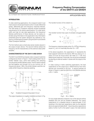
  • 1. Frequency Peaking Compensation of the GX414 and GX424 by J. Ian Ridpath, Senior Applications Engineer, Video/Broadcast Products APPLICATION NOTE INTRODUCTION In video switching applications, the crosspoint switch must The transfer function of this network is: meet several critical specifications which include differential 1 phase, differential gain and frequency response flatness. Vo LC .......1 The GX4 family of crosspoint switches exceed broadcast Ts = = requirements for the above specifications. For wide band- Vi s2 + s R + 1 L LC width and high bit rate data applications, the frequency/ This transfer function has a pair of complex conjugate poles flatness performance of these devices can be easily ex- with tended using information in this application note. Information 1 fo = ....... 2 presented gives the system designer two methods of fre- 2 LC quency compensating a system using the GX414 and GX424 1 L Video Crosspoint Switches. and Q = ....... 3 R C The first method uses a small value series resistor placed in the output of each device. The second method utilises the The frequency response peaks when Q >1/√2 at a frequency frequency roll-off characteristics of the external video buffer equal to fo, but it is maximally flat when Q = 1/√2. amplifier. In the above equations, the capacitance C, represents the CHARACTERISTICS OF THE GX414 AND GX424 load capacitor external to the device. With any value of C, a value of R can be found which will make Q = 1/√2, thus The GX414 and GX424 are bipolar video crosspoint switches flattening the response. Practically, this can be accomplished configured as shown in Figure 1. Each analog switch has an by placing an external resistor in series with the output of the emitter follower input, some level shifting and clamping device. circuits and an emitter follower output. The four switch outputs are tied together and brought out to one common pin. At In video routing or matrix switching applications, the load frequencies above 1 MHz, the emitter follower switches nat- capacitance on the output bus is determined by how many urally exhibit frequency response peaking. devices are connected to the bus. A typical example as shown in Figure 3, uses five GX414s or five GX424s wired as +Vcc a 20 x 1 matrix. CS IN 1 1 TO OUTPUT BUFFER IN OUT 2 5 - GX414's CS #2 3 CS 3 mA #3 CL = 4 x 15pF #4 = 60pF 4 -VEE 5 Fig.1 Enabled Crosspoint Equivalent Circuit IN 20 The output impedance is roughly modelled as shown in Fig. Fig.3 20 x 1 Matrix L R VO For any single selected crosspoint, four of the devices will be + 44 Ω 180 nH disabled and one will be enabled (selected). The output Vi CLOAD capacitance of a disabled device is approximately 15 pF resulting in the total load capacitance seen by the selected device as approximately 60 pF. Assuming stray capacitance adds a further 5 pF to the system output, the total external Fig.2 Output Impedance Model 510 - 39 - 00
  • 2. Method 1. Adding Series Resistance to the Output Using equation 3), the value of R which will cause Q to equal Precise modelling has been done yielding far more accurate 1/√2 will be; results. The effect on the frequency response of any seriescom- R = ( √2 ) . √180 nH pensating resistor can be computer simulated using these ohms √65pF models. Figure 6 is an engineer-generated model of the which yields; R = 74.4 ohms GX414 or GX424 device. This model has been simulated using 'PSpice' (software by MicroSim Corporation) and com- Since the equivalent series output resistance of the device is pared to measured results. A PSpice NETLIST is available on 44 Ω (as shown in Figure 2), an additional 30.4 Ω must be floppy disk from Gennum for assisting the systems engineer added in series with the output in order to make the total and designer. The input and output impedance parameters resistance equal to 74.4 Ω. Figure 4 shows the frequency are specified for frequencies up to 70 or 80 MHz and will response of the above set-up along with the uncompensated produce accurate frequency response results for load ca- response. For this graph, a 33 Ω resistor was used and a 60 pacitances between 10 pF and 100 pF. pF load capacitor simulated the additional disabled devices. IN 100 12 70n 12 12 76n OUT 12 2.5 50p 2.0 0.4 p 100 100 50p RS = 0 Ω 2K 2.5p V1 V2 1.5 CL = 60 pF 1.5 p + 20p + 50p 21p 14p 1.0 125 0.1p V1 40 100 2.2 p 0.998 x V2 20 0.5 1.74 M 2K 2.5p GAIN (dB) 0 -0.5 R = 33Ω -1.0 S Fig. 6 Engineer-generated Model of GX414 or GX424 -1.5 Figure 7 is an approximate model of a disabled crosspoint -2.0 switch showing some of the circuit potentials and more -2.5 importantly, the various capacitances associated with a disa- 0 10 100 bled switch. FREQUENCY (MHz) Fig. 4 Frequency and Uncompensated Responses +8 With the same 33 Ω resistor in the circuit, the load capacitors 600 Ω were changed to 47 pF and 27 pF in order to see their effects on the frequency response. The 47pF capacitor closely V IN + 0.65 V simulates a 16 x 1 crosspoint circuit while the 27 pF approxi- 0.7pF 0.7pF 0.7pF mates a 10 x 1 situation. Figure 5 shows the results of these changes. 0.7pF 1.5pF 1.2K 2pF V OUT 2.5 + 16pF 2.0 1.3 V 12pF 1.5 ´ 1.0 RS = 33 Ω 27 pF GAIN (dB) 0.5 Fig. 7 Disabled Crosspoint Equivalent Circuit 0 47 pF The input capacitance of a disabled switch varies with the DC -0.5 bias voltage from 2.1 pF at -1 volt to 2.5 pF at +1.5 volts. -1.0 Futhermore, there is a slight change in CIN between the disabled state ( 2.2 pF at 0 volts bias ) and enabled state ( 2.0 -1.5 pF at 0 volts bias ). The slight variations would only be -2.0 significant if the input driver source impedance is high. The -2.5 output capacitance of the disabled chip is made up of four 0 10 100 times 0.7 pF, for the four output transistors, plus 12 pF which FREQUENCY (MHz) is common to all outputs, giving a total of approximately 15 pF. Fig. 5 Frequency Responses due to a Change of Capacitor Values 510 - 39 - 00
  • 3. Method 2. Frequency Compensation by the Output Buffer Stage. The only drawback of using a series resistor to compensate for Figure 8 shows a 16 x 1 system that is set up using four GX414's the peaking response of the GX414 and GX424 is the slight and two popular buffer amplifiers. The first is an Elantec EL- degredation of differential phase through the switch and resis- 2020 and the second is a Signetics NE-5539. The EL-2020 is tor. Since the outputs are eventually buffered at the bus by an a 50 MHz current feedback amplifier specifically designed for operational amplifier or a specifically designed video buffer, it use in video applications. The NE-5539 is an ultra-wideband seems reasonable to compensate at this point in the system. operational amplifier having an external frequency compensation pin. INPUTS FOUR GX414s BINARY ADDRESS 0.1 +8V DECODER 1 IN 0 14 V0 +V 2 13 A0 GND A0 3 IN 1 A 1 12 A1 V1 4 GND CS 11 5 10 V2 IN 2 OUT 6 9 GND NC 7 -V 8 V3 IN 3 4 3 0.1 A2 75 75 75 75 -8V 5 1 2 2 A3 +8V 6 74HC139 1 0.1 ENABLE 7 V4 1 IN 0 +V 14 2 GND A 0 13 V5 3 IN 1 A 1 12 LOGIC Vcc < 5V 4 11 GND CS 5 10 V6 IN 2 OUT 6 GND NC 9 V7 7 IN 3 -V 8 0.1 +8V 75 75 75 75 -8V 5 - 70pF 0.1 0.1 +8V 330 12 1 + 10 1 IN 0 14 75 V8 +V NE5539 2 GND 13 2-10pF 14 A0 - 3 3 12 7 V9 IN 1 A1 470 4 82 GND CS 11 FREQ. V 10 5 10 IN 2 OUT COMP. 6 9 GND NC 22 7 -V 8 0.1 V 11 IN 3 75 75 0.1 -8V 75 75 100 GAIN -8V 0.1 +8V +8V 1 14 V 12 IN 0 +V 2 13 0.1 GND A 0 3 12 V 13 IN 1 A1 330 4 GND 11 3 7 CS + 75 5 IN 2 10 EL2020 6 V14 OUT 2 6 GND 9 2-10pF - 4 NC 7 8 V15 IN 3 -V 680 FREQ. 75 0.1 COMP. 75 75 75 330 -8V 0.1 -8V 500 GAIN NOTES Pin 9 is NC ( no connection - pin is floating). Unless otherwise shown all capacitors are in µF and all resistors are in ohms. Fig. 8 16 x 1 Video Crosspoint Circuit 510 - 39 - 00
  • 4. Several combinations of resistor values were used in order to adjusted to flatten the frequency response. The frequency set the gain of each amplifier to 6 dB and yet maintain stability. response was observed and measured using the test set-up A small trimmer capacitor in conjunction with a series resistor as shown in Figure 9. was used as a lag-circuit at the amplifier input. Along with this circuit, in the case of the NE-5539, a compensating trimmer Initially, the buffer amplifiers were set up having as wide a capacitor was connected to the compensation pin. bandwidth as possible. Results approaching those shown in the manufacturer's data book were achieved. The crosspoint Each buffer amplifier was then independently connected to the switches were then placed in the circuit and obvious amounts 16 x 1 crosspoint circuit and the variable circuit elements were of frequency peaking were noticed. ADDRESS 701 ADDRESS 723 HP IB ADDRESS 706 INPUT HP3478A HP2225A DIGITAL MULTIMETER PRINTER BNC CABLE CONNECTOR J1 HP59301A HP8754A ASCII-TO-PARELLEL NETWORK MAG/PHASE CONVERTER ANALYZER OUTPUT 08748-60006 HP9816 DESK COMPUTER PROGRAMMING 50Ω TERMINATION CONNECTORS 8120-2883 REFERENCE PLANE EXTENSION CABLE PROGRAMMING CONNECTOR HP8748A S-PARAMETER DUT TEST SET ADDRESS 707 HP8656A SIGNAL GENERATOR Fig. 9 Test Set-up 510 - 39 - 00
  • 5. 6 The lag-circuit trimmer, the compensating trimmer and gain potentiometers were adjusted until a flat response was achiev- ed. Figures 10, 11 and 12 show the various frequency response 4 results. 2 6 GAIN (dB) 0 4 5539 2020 -2 2 GAIN (dB) 5539 -4 0 0 10 100 2020 FREQUENCY (MHz) -2 Fig. 12 Resultant Flat Response Virtually all peaking has been removed, resulting in a flat -4 response to at least 35 MHz for the NE5539 and at least 15 MHz 0 10 100 for the EL-2020. FREQUENCY (MHz) Fig. 10 Amplifier Response CONCLUSION This brief application note has dealt with the compensation for The wide bandwidth of the NE5539 is obvious with a -3dB flatness that is necessary when using the GX414 and GX424 frequency of well over 200 MHz, while the -3dB point of the EL- video crosspoint switches. The video system designer is 2020 is about 45 MHz. concerned with flatness and insertion loss of any crosspoint switch in his system at the colour burst frequencies of either 3.58 MHz or 4.43 MHz. 6 The insertion loss of the GX4 family of devices at these 5539 4 frequencies in less than 0.05 dB. However, for wideband and high bit rate data, it is important to have a flat response, out to at least 30 to 50 MHz. Using the techniques described in this 2 application note in conjunction with the buffer stages speci- GAIN (dB) fied, the GX414 and GX424 switches can be made to have a 2020 0 flat response up to the frequencies mentioned above. Indeed, the peaking response of the GX414 and GX424 can be -2 used to advantage with a falling response found in most operational amplifier circuits in order to flatten the overall -4 frequency response. 0 10 100 FREQUENCY (MHz) Application engineers at Gennum are more than happy to work along with system designers and will try to answer any customer Fig. 11 Amplifier and Switch Response questions regarding the GX414 and GX424, high performance Video Crosspoint Switches. Predictable peaking occurs in both systems between 40 and 50 MHz. Gennum Corporation assumes no responsibility for the use of any circuits described herein and makes no representations that they are free from patent infringement. ©Copyright August 1989 Gennum Corporation. All rights reserved. Printed in Canada. 510 - 39 - 00