TrustArc Webinar - Stay Ahead of US State Data Privacy Law Developments
M62502FPのデータシート
1. Y n. e. MITSUBISHI (Dig./Ana. INTERFACE)
A L cificacttioto chang
I N pe
I M final s subje
E L is noct lamits are
R is i M62502FP
P ces;Thametri
i r
Not me pa PWM IC for the synchronized deflection system control
So
GENERAL DESCRIPTION
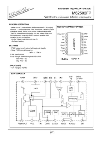
The M62502 is a controller for a deflection system of CRT display PIN CONFIGURATION(TOP VIEW)
monitors. It performs a stable PWM control over a wide fluctuation
of external signals, thanks to the built-in trigger mode oscillator.
The IC is suitable for an application to a high voltage drive and a PWM OUT 1 16 GND
horizontal output correction of CRT monitors because of its
following circuits and functions; Vcc 2 15 VREF
M62502FP
• Under Voltage Lock Out circuit (UVLO) TIN 3 14 DTC
• Soft-start function
Cosc 4 13 FB
FEATURES Cagc1 5 12 IN –
• PWM output synchronized with external signals Ragc 6 11 IN +
• Wide PWM control frequency Cagc2 7 10 Duty
15kHz to 150kHz
2fh 8 9 DOUT
• Soft start function
• Low voltage malfunction protection circuit
start Vcc > 9V Outline 16P2N-A
stop Vcc < 6V
APPLICATION
• C R T display monitor
BLOCK DIAGRAM
Duty DRIVE
GND VREF DTC FB IN- IN+ Adj OUTPUT
16 15 14 13 12 11 10 9
VCC
VREF Duty
Amp
cont
Comp
Wind comp
Comp
UVLO
GEN AGC Edge
GEN AGC detection
1 2 3 4 5 6 7 8
PWM OUT VCC TIN COSC CAGC1 RAGC CAGC2 2fh
(1/7)
2. Y n. e. MITSUBISHI (Dig./Ana. INTERFACE)
A L cificacttioto chang
I N pe
I M final s subje
E L is noct lamits are
R is i M62502FP
P ces;Thametri
i r
Not me pa PWM IC for the synchronized deflection system control
So
Terminal Number and The facility
PIN No. Symbol Functional Description
1 PWM OUT PWM output
2 VCC Power supply
3 TIN Trigger input
4 COSC Setting oscillating frequency
5 Cagc1 AGC setting
6 RAGC AGC Current setting resistor connected to this terminal
7 Cagc2 AGC setting
8 2fh Double velocity reshuffle
9 DOUT Drive output
10 Duty Duty regulation
11 IN+ Positive input of Op-Amp.
12 IN- Negative input of Op-Amp.
13 FB Output of Op-Amp.
14 DTC Dead time control (Soft start function)
15 VREF Output of reference voltage (5V)
16 GND Ground
Absolute Maximum Rating (Ta=25°C,unless otherwise noted)
Symbol Parameter Conditions Ratings Unit
VCC Supply voltage 15 V
VOUT Output voltage 15 V
IOUT Output current ±100 mA
Vd Drive output voltage 15 V
Id Drive output current 20 mA
VICM Error amplifier input common V
mode voltage range -0.3 to VCC
VID Error amplifier input common VCC V
mode voltage
Pd Power dissipation 650 mW
K Thermal derating ratio Ta≥25°C 5.2 mW/°C
Topr Operating ambient temperature -20 to +75 °C
Tstg Storage temperature -40 to +150 °C
(2/7)
3. Y n. e. MITSUBISHI (Dig./Ana. INTERFACE)
A L cificacttioto chang
I N pe
I M final s subje
E L is noct lamits are
R is i M62502FP
P ces;Thametri
i r
Not me pa PWM IC for the synchronized deflection system control
So
ELECTRICAL CHARACTERISTICS (Vcc=12V, TIN=40kHz, Ta=25°C, unless otherwise noted)
Limits
Block Symbol Parameter Test conditions Unit
Min Typ Max
VCC Range of power supply VCC OFF 14 V
ICC Circuit current Output off mode 25 mA
VREF Reference voltage 4.80 5.00 5.20 V
Reg-in Input regulation 1.0 10 mV
Reference
voltage Reg-L Load regulation 2.0 20 mV
section TCVREF Reference voltage thermal coefficient 0.01 %/°C
IREF MAX Maximum reference current -30 mA
IS Short-circuit current -30 mA
VIO Input offset voltage 7 mV
IIb Input bias current -100 nA
IIO Input offset current -100 100 nA
Error VICM Common mode input voltage range -0.3 VCC-2 V
Amp. AV Open loop transmission gain 70 110 dB
SR Slew rate 4 V/µs
VOR Output voltage range 0.3 VREF-1.5 V
Isink Output sink current 10 mA
Isourse Output source current -10 mA
fOSC Oscillation frequency 15 150 kHz
VOSC H The oscillator waveform bound voltage 3.5 V
Oscillator VOSC L The oscillator waveform lower limit voltage 1.5 V
VTIN H High level of TIN 2.5 VCC V
VTIN L Low level of TIN 1.0 V
PWM
output
Vsat L Output saturation voltage L IO=100mA 0.7 1.4 V
section Vsat H Output saturation voltage H IO=-100mA 9.5 10.5 V
UVLO VTH ON ON threshold voltage 8.0 9.0 10.0 V
section VTH OFF OFF threshold voltage 5.4 6.0 6.6 V
Duty adj IDuty Input current VDuty=2.5V -6.5 -1.3 - µA
section Duty max Maximum ON duty VDuty=3V 5.0 µsec
UVP VUVPO Input offset voltage Id=10mA 0.4 V
section IIN UVP UVP terminal input current VDO=12V 1.0 µA
fh reshuffle Ifh fh terminal current Vhf=5V - 330 430 µA
section Vfh fh reshuffle voltage 0.4VREF 0.5VREF 0.6VREF V
(3/7)
4. Y n. e. MITSUBISHI (Dig./Ana. INTERFACE)
A L cificacttioto chang
I N pe
I M final s subje
E L is noct lamits are
R is i M62502FP
P ces;Thametri
i r
Not me pa PWM IC for the synchronized deflection system control
So
Terminal functional description and equivalent circuit
Terminal No. Symbol Function and internal circuit
PWM output 2 Vcc
• PWM output synchronized with the TIN input is available.
• Output "H" level = 10.5V typ
(The output current:-100mA,Vcc=12V) PWM
1 PWM OUT • Output "L" level = 0.7V Typ
1 OUT
(The output current:+100mA,Vcc=12V)
16 GND
2 Vcc Power supply
Vcc 2 15 VREF
Trigger input
• Frequency range
15kHz to 150kHz
• It is taken on a leading edge.
TIN 3
TIN input waveform
3 TIN MIN 2.5V
MAX 1.0V
16 GND
A saw-wave oscillator timing setting (Cosc)
• A saw-wave is generated by connecting the capacitor between pin4 and GND.
• Recommended capacitor value is 1000pF.
Setting AGC sensitivity (Cagc)
• The sensitivity of AGC circuit is set by connecting the capacitor between pin5
4 Cosc and GND.
• Recommended capacitor value is 1µF.
VREF
15
5 Cagc1
Cosc 4 ~
~
5 Cagc1
~
GND 16
(4/7)
5. Y n. e. MITSUBISHI (Dig./Ana. INTERFACE)
A L cificacttioto chang
I N pe
I M final s subje
E L is noct lamits are
R is i M62502FP
P ces;Thametri
i r
Not me pa PWM IC for the synchronized deflection system control
So
Terminal No. Symbol Function and internal circuit
VREF
AGC current setting
• The resistor is connected between pin6 and GND for
setting AGC current flowing in DOUT circuit.
6 Ragc
Ragc 6
VREF
Setting AGC sensitivity
• The sensitivity of AGC is set by connecting
the capacitor between pin7 and GND.
• Recommended capacitor value is 1µF.
7 Cagc2
Cagc2 7
Frequency selection
VREF
• The frequency of drive output is alternated
between just(fh) and doubled(2fh) one.
8 2fh 2fh 8
~
OPEN, GND : fh
VREF : 2fh
~ ~
VREF
Drive output
• Open collector circuit.
9 DOUT
9 DOUT
VREF
The duty adjustment of drive output
10 Duty
Duty 10
(5/7)
6. Y n. e. MITSUBISHI (Dig./Ana. INTERFACE)
A L cificacttioto chang
I N pe
I M final s subje
E L is noct lamits are
R is i M62502FP
P ces;Thametri
i r
Not me pa PWM IC for the synchronized deflection system control
So
Terminal No. Symbol Function and internal circuit
Vcc 2
Positive input of Op-Amp (IN+)
11 IN+
Negative input of OP Amp (IN-)
12 IN-
IN+ 11 12 IN-
Output of Op-Amp (FB)
Dead time control (DTC)
• A soft start function is available during power-on by adopting 15 VREF
a time constant.
13 FB DTC 14
Cosc
FB 13 4
14 DTC
PWM comparator section GND
16
Reference voltage terminal Vcc 2
• 5V is output via this terminal.
A current capability is 5mA.
15 VREF 15 VREF
-
+
GND 16
16 GND • Ground
(6/7)
7. Y n. e. MITSUBISHI (Dig./Ana. INTERFACE)
A L cificacttioto chang
I N pe
I M final s subje
E L is noct lamits are
R is i M62502FP
P ces;Thametri
i r
Not me pa PWM IC for the synchronized deflection system control
So
M62502 application IN- IN+
R2 R3 Duty Vcc
VR1 C3
C5 R5
C2 R1
C4 R4 DOUT
D1
16 15 14 13 12 11 10 9
VCC
VREF Duty
Amp
cont
Comp
Wind
comp
Comp
UVLO
GEN AGC Edge
detection
GEN AGC
Vcc
1 2 3 4 5 6 7 8
Cosc Cagc1 Cagc2
Ragc
PWM OUT TIN 2fh
C1
C1,C2 ----------- These capacitors are for stabilization of Vcc and VREF.
VR1 ----------- It is decided considering a current capability of VREF. (The capability is about 5mA.)
Recommended value is around 10kΩ
C3,D1 ----------- They are for a soft start function. A time constant is decided considering VR1.
Cagc1,2 ----------- These capacitors are for stabilization of AGC circuit. A larger capacitor improves a
stability of the system, however a system response is degraded.
Recommended capacitor value is around 1µF.
Cosc ---------- This capacitor is for the saw-wave generation.
Recommended capacitor value is around 1000pF.
R1,R2,R3,R4 ----- They are for the gain setting of the error Amp. R2 should be several kΩ to dozens of kΩ
C4,C5 to set a voltage gain 20dB to 40dB at f = 1kHz, so that the feed back loop is stable.
When the voltage gain is too low, it causes jitter.
Recommended values of C4, C5 and R1 are ; C4 = dozens of pF to several hundreds pF,
C5 = several thousands pF to tens of thousands pF, R1 = dozens of kΩ to several
hundreds kΩ.
Ragc ----------- This resistor is for the AGC setting of DOUT. Recommended value is 27kΩ.
R5 ----------- It is a pull-up resister of DOUT output, because DOUT is configured by the open
collector circuit. Recommended value is several kΩ.
(7/7)
8. This datasheet has been download from:
www.datasheetcatalog.com
Datasheets for electronics components.