SlideShare uma empresa Scribd logo
1 de 20
Microcontroller 8051

Input/output Pins, Ports & Circuits


                   Rohith.P.N
                   IV th Sem ECE ‘B’ Sec
• As we know Microprocessor doesn't have inbuilt
  Input/output ports.
• It must add an additional chip to interface with the
  external circuitry/devices.

• This disadvantage is overcome by the Microcontroller
  8051.
• MC 8051 has inbuilt I/O ports/circuits.
• This helps the MC 8051 to connect with the external
  devices/memory etc..
Pin Description of the 8051
         P1.0   1           40   Vcc
         P1.1   2           39   P0.0(AD0)
         P1.2   3           38   P0.1(AD1)
         P1.3
         P1.4
                4
                5
                     8051   37
                            36
                                 P0.2(AD2)
                                 P0.3(AD3)
         P1.5   6           35   P0.4(AD4)
         P1.6   7           34   P0.5(AD5)
         P1.7   8           33   P0.6(AD6)
          RST   9           32   P0.7(AD7)
  (RXD)P3.0     10          31   EA/VPP
  (TXD)P3.1     11          30   ALE/PROG
 (INT0)P3.2     12          29   PSEN
 (INT1)P3.3     13          28   P2.7(A15)
     (T0)P3.4   14          27   P2.6(A14)
     (T1)P3.5   15          26   P2.5(A13)
   (WR)P3.6     16          25   P2.4(A12)
    (RD)P3.7    17          24   P2.3(A11)
       XTAL2    18          23   P2.2(A10)
       XTAL1    19          22   P2.1(A9)
         GND    20          21   P2.0(A8)
Pin details of MC 8051
The Microcontroller 8051 has 40 Pins.

I/O Port 0   Pins 32-37
I/O Port 1   Pins 1-8
I/O Port 2   Pins 21-28
I/O Port 3   Pins 10-17

Pin 40 - Vcc
Pin 20 - Gnd
Pin 19 & 18 – XTAL1 & XTAL2
Pin 9 – Reset
Pin 31 – EA (External Access)
Pin 29 – PSEN ( Program Store Enable)
Pin 30 – ALE (Address Latch Enable)
• Vcc(pin 40):
  – Vcc provides supply voltage to the chip.
  – The voltage source is +5V.
• GND(pin 20):ground
• XTAL1 and XTAL2(pins 19,18)
• RST(pin 9):reset
   – It is an input pin and is active high(normally low).
       • The high pulse must be high at least 2 machine cycles.
   – It is a power-on reset.
       • Upon applying a high pulse to RST, the
         microcontroller will reset and all values in registers
         will be lost.
       • Reset values of some 8051 registers
RESET Value of Some 8051 Registers:


Register                Reset Value
PC                      0000
ACC                     0000
B                       0000
PSW                     0000
SP                      0007
DPTR                    0000
RAM are all zero.
• /EA(pin 31):external access
   – There is no on-chip ROM in 8031 and 8032 .
   – The /EA pin is connected to GND to indicate the code is
     stored externally.
   – /PSEN & ALE are used for external ROM.
   – For 8051, /EA pin is connected to Vcc.
   – “/” means active low.
• /PSEN(pin 29):program store enable
   – This is an output pin and is connected to the OE pin of the
     ROM.
• ALE(pin 30):address latch enable
   – It is an output pin and is active high.
   – 8051 port 0 provides both address and data.
   – The ALE pin is used for de-multiplexing the address
     and data by connecting to the G pin of the 74LS373
     latch.
• I/O port pins
   – The four ports P0, P1, P2, and P3.
   – Each port uses 8 pins.
   – All I/O pins are bi-directional.
• The 8051 has four I/O ports
   – Port 0 (pins 32-39):P0(P0.0~P0.7)
   – Port 1(pins 1-8) :P1(P1.0~P1.7)
   – Port 2(pins 21-28):P2(P2.0~P2.7)
   – Port 3(pins 10-17):P3(P3.0~P3.7)
   – Each port has 8 pins.
      • Named P0.X (X=0,1,...,7), P1.X, P2.X, P3.X
      • Ex:P0.0 is the bit 0(LSB)of P0
      • Ex:P0.7 is the bit 7(MSB)of P0
      • These 8 bits form a byte.
• Each port can be used as input or output (bi-direction).
Port
Pin Circuit
Port 0 :-
• When used as input,a ‘1’ must be written to
  corresponding port latch
• Used as an output,’0’ must be be programmed
• Logic ‘1’ in address bit will turn Upper FET on & lower FET
  off
• After address has formed & latched into External circuitry
  by ALE pulse,the External Bus is turned ON
• Port 0 now reads data from External Memory
• Port 0 pins can be accessed by address P0.0,P0.1,….,P0.7
• It can also be addressed as AD0,AD1,…….AD7
Port 0 with Pull-Up Resistors
Port 1 :-

• Port 1 pins have no Dual functions
• If used as input a ‘1’ is written to latch which
  turns upper FET on
• Used as output,lower FET is On & the Pullup is Off
• Output latch is directly connected to gate of
  Lower FET
• Port 1 can be accessed as P1.0,P1.1,. . . . .P1.7
Port 2 :-
• It can be used as i/p or o/p which is similar in operation of
   Port 1
• The alternate use of port 2 is to supply a high-order
   address byte in conjunction with port 0 low-order byte to
   address external memory
• Port 2 latches remain stable when External Memory is
   addressed
• They do not have to be turned around (Set to 1)
  For Data i/p as in Port 0
• It can be accessed as P2.0,P2.1,. . . . . ,P2.7
Port 3 :-
• It is similar to port 1,but has alternate Uses
• Each pin may be individually Programmed as I/O
  or for alternate Functions as shown
       Pin         Alternate Use                 SFR
       P3.0-RXD    Serial data input             SBUF
       P3.1-TXD    Serial data Output            SBUF
       P3.2-INT0   External interrupt 0          TCON.1
       P3.3-INT1   External interrupt 1          TCON.3
       P3.4-T0     External timer 0 input        TMOD
       P3.5-T1     External timer 1 input        TMOD
       P3.6-WR     External Memory Write Pulse    -
       P3.7-RD     External Memory Read Pulse     -
Writing “1” to Output Pin P1.X

      Read latch                              Vcc
                                TB2
                                                    Load(L1)   2. output pin is
1. write a 1 to the pin                                              Vcc
                                      1                            P1.X
     Internal CPU         D     Q
          bus              P1.X                                     pin
                                          0                     output 1
     Write to latch       Clk   Q                   M1


                                    TB1
       Read pin

                                              8051 IC
Writing “0” to Output Pin P1.X

      Read latch                              Vcc
                                TB2
                                                    Load(L1)   2. output pin is
1. write a 0 to the pin                                            ground
                                      0                            P1.X
     Internal CPU         D     Q
          bus              P1.X                                     pin
                                          1                     output 0
     Write to latch       Clk   Q                   M1


                                    TB1
       Read pin

                                              8051 IC
Reading “High” at Input Pin

        Read latch                                   Vcc                 2. MOV A,P1
                                           TB2                         external pin=High
1.   write a 1 to the pin MOV                               Load(L1)
             P1,#0FFH

                                                 1                1        P1.X pin
     Internal CPU bus           D      Q
                                    P1.X
                                                 0         M1
       Write to latch           Clk    Q


                                           TB1
          Read pin
3. Read pin=1 Read latch=0
      Write to latch=1
                                                       8051 IC
Reading “Low” at Input Pin

           Read latch                                 Vcc                2. MOV A,P1
                                            TB2
   1.     write a 1 to the pin                               Load(L1)   external pin=Low
         MOV P1,#0FFH
                                                  1                0        P1.X pin
        Internal CPU bus         D      Q
                                     P1.X
                                                  0         M1
         Write to latch          Clk    Q


                                            TB1
          Read pin
3. Read pin=1 Read latch=0
      Write to latch=1
                                                        8051 IC

Mais conteúdo relacionado

Mais procurados

Addressing modes of 8051
Addressing modes of 8051Addressing modes of 8051
Addressing modes of 8051SARITHA REDDY
 
Digital electronics logic families
Digital electronics logic familiesDigital electronics logic families
Digital electronics logic familiesBLESSINAR0
 
Introduction to Counters
Introduction to CountersIntroduction to Counters
Introduction to CountersISMT College
 
8051 Microcontroller PPT's By Er. Swapnil Kaware
8051 Microcontroller PPT's By Er. Swapnil Kaware8051 Microcontroller PPT's By Er. Swapnil Kaware
8051 Microcontroller PPT's By Er. Swapnil KawareProf. Swapnil V. Kaware
 
8051 architecture
8051 architecture8051 architecture
8051 architecturesb108ec
 
Interfacing adc
Interfacing adcInterfacing adc
Interfacing adcPRADEEP
 
Keypad Interfacing with 8051 Microcontroller
Keypad Interfacing with 8051 MicrocontrollerKeypad Interfacing with 8051 Microcontroller
Keypad Interfacing with 8051 MicrocontrollerSudhanshu Janwadkar
 
555 Timer (detailed presentation)
555 Timer (detailed presentation)555 Timer (detailed presentation)
555 Timer (detailed presentation)Tanish Gupta
 
8051 microcontroller
8051 microcontroller 8051 microcontroller
8051 microcontroller Gaurav Verma
 
Question paper with solution the 8051 microcontroller based embedded systems...
Question paper with solution  the 8051 microcontroller based embedded systems...Question paper with solution  the 8051 microcontroller based embedded systems...
Question paper with solution the 8051 microcontroller based embedded systems...manishpatel_79
 
DAC Interfacing with 8051.pdf
DAC Interfacing with 8051.pdfDAC Interfacing with 8051.pdf
DAC Interfacing with 8051.pdfSrikrishna Thota
 

Mais procurados (20)

Shift Registers
Shift RegistersShift Registers
Shift Registers
 
Addressing modes of 8051
Addressing modes of 8051Addressing modes of 8051
Addressing modes of 8051
 
Digital electronics logic families
Digital electronics logic familiesDigital electronics logic families
Digital electronics logic families
 
8051 ch9-950217
8051 ch9-9502178051 ch9-950217
8051 ch9-950217
 
Serial Communication in 8051
Serial Communication in 8051Serial Communication in 8051
Serial Communication in 8051
 
Introduction to Counters
Introduction to CountersIntroduction to Counters
Introduction to Counters
 
8051 Microcontroller PPT's By Er. Swapnil Kaware
8051 Microcontroller PPT's By Er. Swapnil Kaware8051 Microcontroller PPT's By Er. Swapnil Kaware
8051 Microcontroller PPT's By Er. Swapnil Kaware
 
8051 architecture
8051 architecture8051 architecture
8051 architecture
 
Interfacing adc
Interfacing adcInterfacing adc
Interfacing adc
 
Keypad Interfacing with 8051 Microcontroller
Keypad Interfacing with 8051 MicrocontrollerKeypad Interfacing with 8051 Microcontroller
Keypad Interfacing with 8051 Microcontroller
 
8051 i/o port circuit
8051 i/o port circuit8051 i/o port circuit
8051 i/o port circuit
 
555 Timer (detailed presentation)
555 Timer (detailed presentation)555 Timer (detailed presentation)
555 Timer (detailed presentation)
 
Ring counter
Ring counterRing counter
Ring counter
 
8051 microcontroller
8051 microcontroller 8051 microcontroller
8051 microcontroller
 
Adc interfacing
Adc interfacingAdc interfacing
Adc interfacing
 
DAC and sensor interfacing with PIC
DAC and sensor interfacing with PICDAC and sensor interfacing with PIC
DAC and sensor interfacing with PIC
 
8051 MICROCONTROLLER
8051 MICROCONTROLLER 8051 MICROCONTROLLER
8051 MICROCONTROLLER
 
8255 PPI
8255 PPI8255 PPI
8255 PPI
 
Question paper with solution the 8051 microcontroller based embedded systems...
Question paper with solution  the 8051 microcontroller based embedded systems...Question paper with solution  the 8051 microcontroller based embedded systems...
Question paper with solution the 8051 microcontroller based embedded systems...
 
DAC Interfacing with 8051.pdf
DAC Interfacing with 8051.pdfDAC Interfacing with 8051.pdf
DAC Interfacing with 8051.pdf
 

Destaque

I o ports and timers of 8051
I o ports and timers of 8051I o ports and timers of 8051
I o ports and timers of 8051SARITHA REDDY
 
8051 Microcontroller Notes
8051 Microcontroller Notes8051 Microcontroller Notes
8051 Microcontroller NotesDr.YNM
 
8051 Timers / Counters
8051 Timers / Counters8051 Timers / Counters
8051 Timers / CountersPatricio Lima
 
8051 Timers and Counters
8051 Timers and Counters8051 Timers and Counters
8051 Timers and CountersShreyans Pathak
 
Input output ports and connectors
Input output ports and connectorsInput output ports and connectors
Input output ports and connectorsbhardwaj1992
 
8051 timer counter
8051 timer counter8051 timer counter
8051 timer counterankit3991
 
Architecture of 8051 microcontroller))
Architecture of 8051 microcontroller))Architecture of 8051 microcontroller))
Architecture of 8051 microcontroller))Ganesh Ram
 
PIC-MICROCONTROLLER TUTORIALS FOR BEGINNERS
PIC-MICROCONTROLLER TUTORIALS FOR BEGINNERSPIC-MICROCONTROLLER TUTORIALS FOR BEGINNERS
PIC-MICROCONTROLLER TUTORIALS FOR BEGINNERSVISHNU KP
 
Ports and connectors
Ports and connectorsPorts and connectors
Ports and connectorschrispaul8676
 
PIC 16F877A by PARTHIBAN. S.
PIC 16F877A   by PARTHIBAN. S.PIC 16F877A   by PARTHIBAN. S.
PIC 16F877A by PARTHIBAN. S.parthi_arjun
 
Wireless transmission of voice signal using nRF24L01 module
Wireless transmission of voice signal using nRF24L01 moduleWireless transmission of voice signal using nRF24L01 module
Wireless transmission of voice signal using nRF24L01 moduleSunil Kumar Shesma
 
Communication systems Projects for Final Year Students
Communication systems Projects for Final Year StudentsCommunication systems Projects for Final Year Students
Communication systems Projects for Final Year StudentsManoj Subramanian
 
Embedded systems and its ports
Embedded systems and its portsEmbedded systems and its ports
Embedded systems and its portsnitin kumar
 

Destaque (20)

I/O Ports
I/O Ports I/O Ports
I/O Ports
 
I o ports and timers of 8051
I o ports and timers of 8051I o ports and timers of 8051
I o ports and timers of 8051
 
8051 Microcontroller Notes
8051 Microcontroller Notes8051 Microcontroller Notes
8051 Microcontroller Notes
 
8051 Timers / Counters
8051 Timers / Counters8051 Timers / Counters
8051 Timers / Counters
 
8051 Timers and Counters
8051 Timers and Counters8051 Timers and Counters
8051 Timers and Counters
 
Microcontroller 8051
Microcontroller 8051Microcontroller 8051
Microcontroller 8051
 
8051 interrupts
8051 interrupts8051 interrupts
8051 interrupts
 
Input output ports and connectors
Input output ports and connectorsInput output ports and connectors
Input output ports and connectors
 
8051 timer counter
8051 timer counter8051 timer counter
8051 timer counter
 
Architecture of 8051 microcontroller))
Architecture of 8051 microcontroller))Architecture of 8051 microcontroller))
Architecture of 8051 microcontroller))
 
Getting started with pic microcontrollers
Getting started with pic microcontrollersGetting started with pic microcontrollers
Getting started with pic microcontrollers
 
PIC-MICROCONTROLLER TUTORIALS FOR BEGINNERS
PIC-MICROCONTROLLER TUTORIALS FOR BEGINNERSPIC-MICROCONTROLLER TUTORIALS FOR BEGINNERS
PIC-MICROCONTROLLER TUTORIALS FOR BEGINNERS
 
Ports and connectors
Ports and connectorsPorts and connectors
Ports and connectors
 
PIC 16F877A by PARTHIBAN. S.
PIC 16F877A   by PARTHIBAN. S.PIC 16F877A   by PARTHIBAN. S.
PIC 16F877A by PARTHIBAN. S.
 
Ch3 ppt
Ch3 pptCh3 ppt
Ch3 ppt
 
MPU-6050_RF24L01
MPU-6050_RF24L01MPU-6050_RF24L01
MPU-6050_RF24L01
 
Wireless transmission of voice signal using nRF24L01 module
Wireless transmission of voice signal using nRF24L01 moduleWireless transmission of voice signal using nRF24L01 module
Wireless transmission of voice signal using nRF24L01 module
 
Communication systems Projects for Final Year Students
Communication systems Projects for Final Year StudentsCommunication systems Projects for Final Year Students
Communication systems Projects for Final Year Students
 
Ch09
Ch09Ch09
Ch09
 
Embedded systems and its ports
Embedded systems and its portsEmbedded systems and its ports
Embedded systems and its ports
 

Semelhante a I o ports.ppt

Semelhante a I o ports.ppt (20)

8051 ports
8051 ports8051 ports
8051 ports
 
Microcontroller 8051
Microcontroller 8051Microcontroller 8051
Microcontroller 8051
 
Microcontroller 8051
Microcontroller 8051Microcontroller 8051
Microcontroller 8051
 
8051 full ppt
8051 full ppt8051 full ppt
8051 full ppt
 
Microcontroller 8051 By Mitesh kumar
Microcontroller 8051 By Mitesh kumarMicrocontroller 8051 By Mitesh kumar
Microcontroller 8051 By Mitesh kumar
 
Microcontroller 8051
Microcontroller 8051Microcontroller 8051
Microcontroller 8051
 
8051microcontroller
8051microcontroller 8051microcontroller
8051microcontroller
 
8051 microcontrollers ch3
8051 microcontrollers ch38051 microcontrollers ch3
8051 microcontrollers ch3
 
Class7
Class7Class7
Class7
 
itft-Microcontriller 8051
itft-Microcontriller 8051itft-Microcontriller 8051
itft-Microcontriller 8051
 
Microcontroller 8051 third
Microcontroller 8051  thirdMicrocontroller 8051  third
Microcontroller 8051 third
 
Datasheet8951
Datasheet8951Datasheet8951
Datasheet8951
 
8051 microcontroller lecture ppt by Tarun Khaneja ( 9034406598 )
8051 microcontroller lecture ppt by Tarun Khaneja ( 9034406598 )8051 microcontroller lecture ppt by Tarun Khaneja ( 9034406598 )
8051 microcontroller lecture ppt by Tarun Khaneja ( 9034406598 )
 
Microcontroller 8051 gs
Microcontroller 8051 gsMicrocontroller 8051 gs
Microcontroller 8051 gs
 
AT89C52 Data sheet
AT89C52 Data sheetAT89C52 Data sheet
AT89C52 Data sheet
 
8051 Microcontroller
8051 Microcontroller8051 Microcontroller
8051 Microcontroller
 
Embedded Systems
Embedded SystemsEmbedded Systems
Embedded Systems
 
At89 c51
At89 c51At89 c51
At89 c51
 
dspAt89 s52
dspAt89 s52dspAt89 s52
dspAt89 s52
 
Intel 8051 - pin description
Intel 8051  - pin descriptionIntel 8051  - pin description
Intel 8051 - pin description
 

Último

Dyslexia AI Workshop for Slideshare.pptx
Dyslexia AI Workshop for Slideshare.pptxDyslexia AI Workshop for Slideshare.pptx
Dyslexia AI Workshop for Slideshare.pptxcallscotland1987
 
Unit-V; Pricing (Pharma Marketing Management).pptx
Unit-V; Pricing (Pharma Marketing Management).pptxUnit-V; Pricing (Pharma Marketing Management).pptx
Unit-V; Pricing (Pharma Marketing Management).pptxVishalSingh1417
 
How to Create and Manage Wizard in Odoo 17
How to Create and Manage Wizard in Odoo 17How to Create and Manage Wizard in Odoo 17
How to Create and Manage Wizard in Odoo 17Celine George
 
1029 - Danh muc Sach Giao Khoa 10 . pdf
1029 -  Danh muc Sach Giao Khoa 10 . pdf1029 -  Danh muc Sach Giao Khoa 10 . pdf
1029 - Danh muc Sach Giao Khoa 10 . pdfQucHHunhnh
 
Holdier Curriculum Vitae (April 2024).pdf
Holdier Curriculum Vitae (April 2024).pdfHoldier Curriculum Vitae (April 2024).pdf
Holdier Curriculum Vitae (April 2024).pdfagholdier
 
This PowerPoint helps students to consider the concept of infinity.
This PowerPoint helps students to consider the concept of infinity.This PowerPoint helps students to consider the concept of infinity.
This PowerPoint helps students to consider the concept of infinity.christianmathematics
 
Basic Civil Engineering first year Notes- Chapter 4 Building.pptx
Basic Civil Engineering first year Notes- Chapter 4 Building.pptxBasic Civil Engineering first year Notes- Chapter 4 Building.pptx
Basic Civil Engineering first year Notes- Chapter 4 Building.pptxDenish Jangid
 
SKILL OF INTRODUCING THE LESSON MICRO SKILLS.pptx
SKILL OF INTRODUCING THE LESSON MICRO SKILLS.pptxSKILL OF INTRODUCING THE LESSON MICRO SKILLS.pptx
SKILL OF INTRODUCING THE LESSON MICRO SKILLS.pptxAmanpreet Kaur
 
How to Give a Domain for a Field in Odoo 17
How to Give a Domain for a Field in Odoo 17How to Give a Domain for a Field in Odoo 17
How to Give a Domain for a Field in Odoo 17Celine George
 
Single or Multiple melodic lines structure
Single or Multiple melodic lines structureSingle or Multiple melodic lines structure
Single or Multiple melodic lines structuredhanjurrannsibayan2
 
2024-NATIONAL-LEARNING-CAMP-AND-OTHER.pptx
2024-NATIONAL-LEARNING-CAMP-AND-OTHER.pptx2024-NATIONAL-LEARNING-CAMP-AND-OTHER.pptx
2024-NATIONAL-LEARNING-CAMP-AND-OTHER.pptxMaritesTamaniVerdade
 
Mixin Classes in Odoo 17 How to Extend Models Using Mixin Classes
Mixin Classes in Odoo 17  How to Extend Models Using Mixin ClassesMixin Classes in Odoo 17  How to Extend Models Using Mixin Classes
Mixin Classes in Odoo 17 How to Extend Models Using Mixin ClassesCeline George
 
Introduction to Nonprofit Accounting: The Basics
Introduction to Nonprofit Accounting: The BasicsIntroduction to Nonprofit Accounting: The Basics
Introduction to Nonprofit Accounting: The BasicsTechSoup
 
Micro-Scholarship, What it is, How can it help me.pdf
Micro-Scholarship, What it is, How can it help me.pdfMicro-Scholarship, What it is, How can it help me.pdf
Micro-Scholarship, What it is, How can it help me.pdfPoh-Sun Goh
 
UGC NET Paper 1 Mathematical Reasoning & Aptitude.pdf
UGC NET Paper 1 Mathematical Reasoning & Aptitude.pdfUGC NET Paper 1 Mathematical Reasoning & Aptitude.pdf
UGC NET Paper 1 Mathematical Reasoning & Aptitude.pdfNirmal Dwivedi
 
Kodo Millet PPT made by Ghanshyam bairwa college of Agriculture kumher bhara...
Kodo Millet  PPT made by Ghanshyam bairwa college of Agriculture kumher bhara...Kodo Millet  PPT made by Ghanshyam bairwa college of Agriculture kumher bhara...
Kodo Millet PPT made by Ghanshyam bairwa college of Agriculture kumher bhara...pradhanghanshyam7136
 
Fostering Friendships - Enhancing Social Bonds in the Classroom
Fostering Friendships - Enhancing Social Bonds  in the ClassroomFostering Friendships - Enhancing Social Bonds  in the Classroom
Fostering Friendships - Enhancing Social Bonds in the ClassroomPooky Knightsmith
 
1029-Danh muc Sach Giao Khoa khoi 6.pdf
1029-Danh muc Sach Giao Khoa khoi  6.pdf1029-Danh muc Sach Giao Khoa khoi  6.pdf
1029-Danh muc Sach Giao Khoa khoi 6.pdfQucHHunhnh
 
Explore beautiful and ugly buildings. Mathematics helps us create beautiful d...
Explore beautiful and ugly buildings. Mathematics helps us create beautiful d...Explore beautiful and ugly buildings. Mathematics helps us create beautiful d...
Explore beautiful and ugly buildings. Mathematics helps us create beautiful d...christianmathematics
 
Accessible Digital Futures project (20/03/2024)
Accessible Digital Futures project (20/03/2024)Accessible Digital Futures project (20/03/2024)
Accessible Digital Futures project (20/03/2024)Jisc
 

Último (20)

Dyslexia AI Workshop for Slideshare.pptx
Dyslexia AI Workshop for Slideshare.pptxDyslexia AI Workshop for Slideshare.pptx
Dyslexia AI Workshop for Slideshare.pptx
 
Unit-V; Pricing (Pharma Marketing Management).pptx
Unit-V; Pricing (Pharma Marketing Management).pptxUnit-V; Pricing (Pharma Marketing Management).pptx
Unit-V; Pricing (Pharma Marketing Management).pptx
 
How to Create and Manage Wizard in Odoo 17
How to Create and Manage Wizard in Odoo 17How to Create and Manage Wizard in Odoo 17
How to Create and Manage Wizard in Odoo 17
 
1029 - Danh muc Sach Giao Khoa 10 . pdf
1029 -  Danh muc Sach Giao Khoa 10 . pdf1029 -  Danh muc Sach Giao Khoa 10 . pdf
1029 - Danh muc Sach Giao Khoa 10 . pdf
 
Holdier Curriculum Vitae (April 2024).pdf
Holdier Curriculum Vitae (April 2024).pdfHoldier Curriculum Vitae (April 2024).pdf
Holdier Curriculum Vitae (April 2024).pdf
 
This PowerPoint helps students to consider the concept of infinity.
This PowerPoint helps students to consider the concept of infinity.This PowerPoint helps students to consider the concept of infinity.
This PowerPoint helps students to consider the concept of infinity.
 
Basic Civil Engineering first year Notes- Chapter 4 Building.pptx
Basic Civil Engineering first year Notes- Chapter 4 Building.pptxBasic Civil Engineering first year Notes- Chapter 4 Building.pptx
Basic Civil Engineering first year Notes- Chapter 4 Building.pptx
 
SKILL OF INTRODUCING THE LESSON MICRO SKILLS.pptx
SKILL OF INTRODUCING THE LESSON MICRO SKILLS.pptxSKILL OF INTRODUCING THE LESSON MICRO SKILLS.pptx
SKILL OF INTRODUCING THE LESSON MICRO SKILLS.pptx
 
How to Give a Domain for a Field in Odoo 17
How to Give a Domain for a Field in Odoo 17How to Give a Domain for a Field in Odoo 17
How to Give a Domain for a Field in Odoo 17
 
Single or Multiple melodic lines structure
Single or Multiple melodic lines structureSingle or Multiple melodic lines structure
Single or Multiple melodic lines structure
 
2024-NATIONAL-LEARNING-CAMP-AND-OTHER.pptx
2024-NATIONAL-LEARNING-CAMP-AND-OTHER.pptx2024-NATIONAL-LEARNING-CAMP-AND-OTHER.pptx
2024-NATIONAL-LEARNING-CAMP-AND-OTHER.pptx
 
Mixin Classes in Odoo 17 How to Extend Models Using Mixin Classes
Mixin Classes in Odoo 17  How to Extend Models Using Mixin ClassesMixin Classes in Odoo 17  How to Extend Models Using Mixin Classes
Mixin Classes in Odoo 17 How to Extend Models Using Mixin Classes
 
Introduction to Nonprofit Accounting: The Basics
Introduction to Nonprofit Accounting: The BasicsIntroduction to Nonprofit Accounting: The Basics
Introduction to Nonprofit Accounting: The Basics
 
Micro-Scholarship, What it is, How can it help me.pdf
Micro-Scholarship, What it is, How can it help me.pdfMicro-Scholarship, What it is, How can it help me.pdf
Micro-Scholarship, What it is, How can it help me.pdf
 
UGC NET Paper 1 Mathematical Reasoning & Aptitude.pdf
UGC NET Paper 1 Mathematical Reasoning & Aptitude.pdfUGC NET Paper 1 Mathematical Reasoning & Aptitude.pdf
UGC NET Paper 1 Mathematical Reasoning & Aptitude.pdf
 
Kodo Millet PPT made by Ghanshyam bairwa college of Agriculture kumher bhara...
Kodo Millet  PPT made by Ghanshyam bairwa college of Agriculture kumher bhara...Kodo Millet  PPT made by Ghanshyam bairwa college of Agriculture kumher bhara...
Kodo Millet PPT made by Ghanshyam bairwa college of Agriculture kumher bhara...
 
Fostering Friendships - Enhancing Social Bonds in the Classroom
Fostering Friendships - Enhancing Social Bonds  in the ClassroomFostering Friendships - Enhancing Social Bonds  in the Classroom
Fostering Friendships - Enhancing Social Bonds in the Classroom
 
1029-Danh muc Sach Giao Khoa khoi 6.pdf
1029-Danh muc Sach Giao Khoa khoi  6.pdf1029-Danh muc Sach Giao Khoa khoi  6.pdf
1029-Danh muc Sach Giao Khoa khoi 6.pdf
 
Explore beautiful and ugly buildings. Mathematics helps us create beautiful d...
Explore beautiful and ugly buildings. Mathematics helps us create beautiful d...Explore beautiful and ugly buildings. Mathematics helps us create beautiful d...
Explore beautiful and ugly buildings. Mathematics helps us create beautiful d...
 
Accessible Digital Futures project (20/03/2024)
Accessible Digital Futures project (20/03/2024)Accessible Digital Futures project (20/03/2024)
Accessible Digital Futures project (20/03/2024)
 

I o ports.ppt

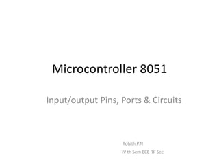
  • 1. Microcontroller 8051 Input/output Pins, Ports & Circuits Rohith.P.N IV th Sem ECE ‘B’ Sec
  • 2. • As we know Microprocessor doesn't have inbuilt Input/output ports. • It must add an additional chip to interface with the external circuitry/devices. • This disadvantage is overcome by the Microcontroller 8051. • MC 8051 has inbuilt I/O ports/circuits. • This helps the MC 8051 to connect with the external devices/memory etc..
  • 3. Pin Description of the 8051 P1.0 1 40 Vcc P1.1 2 39 P0.0(AD0) P1.2 3 38 P0.1(AD1) P1.3 P1.4 4 5 8051 37 36 P0.2(AD2) P0.3(AD3) P1.5 6 35 P0.4(AD4) P1.6 7 34 P0.5(AD5) P1.7 8 33 P0.6(AD6) RST 9 32 P0.7(AD7) (RXD)P3.0 10 31 EA/VPP (TXD)P3.1 11 30 ALE/PROG (INT0)P3.2 12 29 PSEN (INT1)P3.3 13 28 P2.7(A15) (T0)P3.4 14 27 P2.6(A14) (T1)P3.5 15 26 P2.5(A13) (WR)P3.6 16 25 P2.4(A12) (RD)P3.7 17 24 P2.3(A11) XTAL2 18 23 P2.2(A10) XTAL1 19 22 P2.1(A9) GND 20 21 P2.0(A8)
  • 4. Pin details of MC 8051 The Microcontroller 8051 has 40 Pins. I/O Port 0 Pins 32-37 I/O Port 1 Pins 1-8 I/O Port 2 Pins 21-28 I/O Port 3 Pins 10-17 Pin 40 - Vcc Pin 20 - Gnd Pin 19 & 18 – XTAL1 & XTAL2 Pin 9 – Reset Pin 31 – EA (External Access) Pin 29 – PSEN ( Program Store Enable) Pin 30 – ALE (Address Latch Enable)
  • 5. • Vcc(pin 40): – Vcc provides supply voltage to the chip. – The voltage source is +5V. • GND(pin 20):ground • XTAL1 and XTAL2(pins 19,18)
  • 6. • RST(pin 9):reset – It is an input pin and is active high(normally low). • The high pulse must be high at least 2 machine cycles. – It is a power-on reset. • Upon applying a high pulse to RST, the microcontroller will reset and all values in registers will be lost. • Reset values of some 8051 registers
  • 7. RESET Value of Some 8051 Registers: Register Reset Value PC 0000 ACC 0000 B 0000 PSW 0000 SP 0007 DPTR 0000 RAM are all zero.
  • 8. • /EA(pin 31):external access – There is no on-chip ROM in 8031 and 8032 . – The /EA pin is connected to GND to indicate the code is stored externally. – /PSEN & ALE are used for external ROM. – For 8051, /EA pin is connected to Vcc. – “/” means active low. • /PSEN(pin 29):program store enable – This is an output pin and is connected to the OE pin of the ROM.
  • 9. • ALE(pin 30):address latch enable – It is an output pin and is active high. – 8051 port 0 provides both address and data. – The ALE pin is used for de-multiplexing the address and data by connecting to the G pin of the 74LS373 latch. • I/O port pins – The four ports P0, P1, P2, and P3. – Each port uses 8 pins. – All I/O pins are bi-directional.
  • 10. • The 8051 has four I/O ports – Port 0 (pins 32-39):P0(P0.0~P0.7) – Port 1(pins 1-8) :P1(P1.0~P1.7) – Port 2(pins 21-28):P2(P2.0~P2.7) – Port 3(pins 10-17):P3(P3.0~P3.7) – Each port has 8 pins. • Named P0.X (X=0,1,...,7), P1.X, P2.X, P3.X • Ex:P0.0 is the bit 0(LSB)of P0 • Ex:P0.7 is the bit 7(MSB)of P0 • These 8 bits form a byte. • Each port can be used as input or output (bi-direction).
  • 12. Port 0 :- • When used as input,a ‘1’ must be written to corresponding port latch • Used as an output,’0’ must be be programmed • Logic ‘1’ in address bit will turn Upper FET on & lower FET off • After address has formed & latched into External circuitry by ALE pulse,the External Bus is turned ON • Port 0 now reads data from External Memory • Port 0 pins can be accessed by address P0.0,P0.1,….,P0.7 • It can also be addressed as AD0,AD1,…….AD7
  • 13. Port 0 with Pull-Up Resistors
  • 14. Port 1 :- • Port 1 pins have no Dual functions • If used as input a ‘1’ is written to latch which turns upper FET on • Used as output,lower FET is On & the Pullup is Off • Output latch is directly connected to gate of Lower FET • Port 1 can be accessed as P1.0,P1.1,. . . . .P1.7
  • 15. Port 2 :- • It can be used as i/p or o/p which is similar in operation of Port 1 • The alternate use of port 2 is to supply a high-order address byte in conjunction with port 0 low-order byte to address external memory • Port 2 latches remain stable when External Memory is addressed • They do not have to be turned around (Set to 1) For Data i/p as in Port 0 • It can be accessed as P2.0,P2.1,. . . . . ,P2.7
  • 16. Port 3 :- • It is similar to port 1,but has alternate Uses • Each pin may be individually Programmed as I/O or for alternate Functions as shown Pin Alternate Use SFR P3.0-RXD Serial data input SBUF P3.1-TXD Serial data Output SBUF P3.2-INT0 External interrupt 0 TCON.1 P3.3-INT1 External interrupt 1 TCON.3 P3.4-T0 External timer 0 input TMOD P3.5-T1 External timer 1 input TMOD P3.6-WR External Memory Write Pulse - P3.7-RD External Memory Read Pulse -
  • 17. Writing “1” to Output Pin P1.X Read latch Vcc TB2 Load(L1) 2. output pin is 1. write a 1 to the pin Vcc 1 P1.X Internal CPU D Q bus P1.X pin 0 output 1 Write to latch Clk Q M1 TB1 Read pin 8051 IC
  • 18. Writing “0” to Output Pin P1.X Read latch Vcc TB2 Load(L1) 2. output pin is 1. write a 0 to the pin ground 0 P1.X Internal CPU D Q bus P1.X pin 1 output 0 Write to latch Clk Q M1 TB1 Read pin 8051 IC
  • 19. Reading “High” at Input Pin Read latch Vcc 2. MOV A,P1 TB2 external pin=High 1. write a 1 to the pin MOV Load(L1) P1,#0FFH 1 1 P1.X pin Internal CPU bus D Q P1.X 0 M1 Write to latch Clk Q TB1 Read pin 3. Read pin=1 Read latch=0 Write to latch=1 8051 IC
  • 20. Reading “Low” at Input Pin Read latch Vcc 2. MOV A,P1 TB2 1. write a 1 to the pin Load(L1) external pin=Low MOV P1,#0FFH 1 0 P1.X pin Internal CPU bus D Q P1.X 0 M1 Write to latch Clk Q TB1 Read pin 3. Read pin=1 Read latch=0 Write to latch=1 8051 IC