SlideShare uma empresa Scribd logo
1 de 9
Baixar para ler offline
c12) United States Patent
Iwatake et al.
(54) VIA CONTACT STRUCTURE HAVING DUAL
SILICIDE LAYERS
(75) Inventors: Michael M. Iwatake, Wappingers Falls,
NY (US); Kevin E. Mello, Fishkill, NY
(US); Matthew W. Oonk, Poughkeepsie,
NY (US); Amanda L. Piper,
Poughkeepsie, NY (US); Yun Y. Wang,
Poughquag, NY (US); Keith K. Wong,
Wappingers Falls, NY (US)
(73) Assignee: International Business Machines
Corporation, Armonk, NY (US)
( *) Notice: Subject to any disclaimer, the term ofthis
patent is extended or adjusted under 35
U.S.C. 154(b) by 2197 days.
(21) Appl. No.: 10/711,298
(22) Filed: Sep.9,2004
(65) Prior Publication Data
US 2006/0051959 Al Mar. 9, 2006
(51) Int. Cl.
HOJL 23152 (2006.01)
(52) U.S. Cl. ........ 257/384; 257/389; 257/751; 257/757;
257/E29.268
(58) Field of Classification Search .......... 257/750-754,
257/763-764,768-770,384,389, 757,E29.268
See application file for complete search history.
111111 1111111111111111111111111111111111111111111111111111111111111
US008288828B2
(10) Patent No.: US 8,288,828 B2
Oct. 16, 2012(45) Date of Patent:
(56) References Cited
U.S. PATENT DOCUMENTS
5,094,981 A *
5,565,708 A *
5,571,753 A *
5,834,846 A
6,277,729 B1 *
6,613,670 B2 *
6,677,230 B2
3/1992 Chung eta!. .................. 438/621
10/1996 Ohsaki eta!. ................. 257/764
1111996 Saruwatari .................... 438/527
1111998 Shinriki eta!.
8/2001 Wu et a!. ....................... 438/627
9/2003 Rha eta!. ...................... 438/657
112004 Yokoyama eta!.
2002/0019127 A1 212002 Givens
FOREIGN PATENT DOCUMENTS
JP 08-107087 * 4/1996
* cited by examiner
Primary Examiner- Anh Mai
(74) Attorney, Agent, or Firm- Yuanmin Cai
(57) ABSTRACT
A via contact is provided to a diffusion region at a top surface
ofa substrate which includes a single-crystal semiconductor
region. The via contact includes a first layer which consists
essentially of a silicide of a first metal in contact with the
diffusionregion at the top surface. A dielectric region overlies
the first layer, the dielectric region having an outer surface and
an opening extending from the outer surface to the top surface
ofthe substrate. A second layer lines the opening and contacts
the top surface of the substrate in the opening, the second
layer including a second metal which lines a sidewall of the
opening and a silicide of the second metal which is self-
aligned to the top surface of the substrate in the opening. A
diffusion barrier layer overlies the second layer within the
opening. A third layer including a third metal overlies the
diffusion barrier layer and fills the opening.
10 Claims, 3 Drawing Sheets
JOO
1'1-t. !lo ~·~ I'~ ~~!If> /tz.O
~..... '/~ r-
_21_
lo~"-..(
/
f.- IL-'2-
L2::- '
(1 os
/
yiOfo
1/llh
/
-

'.. 0
------
/
,.-
..._.l
{
----.,.,.
o6
03
r---{02
U.S. Patent Oct. 16, 2012 Sheet 1 of 3
JOO
ltb ll ~~1 f~~ 0
.
--..,.,. ,-- liZ
~ /
lol{0
-- 12Y j00
/
/
-I '2"2.. /!lh
/
"
~ l1os
~
' 0
FIG. 2
/
lol
f
)
<......./
FIG. 3
)
US 8,288,828 B2
/120
,...--
.,.
1'---l
I
~
oG
103
,-~ 102
. - lrP
03~
-I
..-- _,
----
'-
lo5
---
~
lo'2
U.S. Patent Oct. 16, 2012 Sheet 2 of 3
FIG. 4 ?lO
jJD-.
~~32..
~tot
FIG. 5 .~ ,10
I
11J)-__
~.--1c~
!32--
~ .J,.
-..
1,atrL,?}i
FIG. 6
ITZ.~
t'-
)-/Db
~/ /
1'
'10
US 8,288,828 B2
-- ...
...
'CS
103
-··I- (02..
~I- 11'2..
.-{02
U.S. Patent Oct. 16, 2012 Sheet 3 of 3 US 8,288,828 B2
FIG. 7
/r-JJD
/
I
11~ 120 ,.. ~
-11-1..- ~ ,~lo0
FIG. 8
/.
to?!
.0
US 8,288,828 B2
1
VIA CONTACT STRUCTURE HAVING DUAL
SILICIDE LAYERS
BACKGROUND OF INVENTION
The present invention relates to integrated circuits and their
fabrication. More specifically, the invention relates to the
structure and fabrication ofa via contact to a diffusion region
at a top surface ofa single-crystal semiconductor region ofa
substrate.
A particular challenge encountered in the fabrication of
integrated circuits is the formation ofmetallic via contacts to
diffusion regions (referred to alternatively as "diffusions") of
semiconductor devices. Such diffusion regions are formed in
single-crystal semiconductor regions ofa substrate, such that
an ohmic contact is made between the metallic material in the
via and the semiconductor material of the diffusion region.
The challenge is particularly difficult to provide a robust
structure and method offorming metallic via contacts having
acceptably low contact resistance between the metal and the
diffusion region, over all chip locations of an entire wafer.
Thus, processes and structures known heretofore have
resulted in acceptable contact resistance, but only when a
sufficiently thick layer of a metal silicide, e.g., greater than
20-25 nm of cobalt silicide (CoSi2 ) or nickel monosilicide
(NiSi), for example, is provided at a top surface ofthe diffu-
sion region. In one such exemplary process, a metal silicide
layer is formed in contact with the diffusion region of the
substrate, after which an interlevel dielectric (ILD) is formed,
typically consisting essentially ofa highly flowable, planariz-
ing dielectric such as borophosphosilicate glass (BPSG),
undoped silicate glass (USG) or silicon dioxide deposited
from a tetraethylorthosilicate (TEOS) precursor.
Thereafter, the ILD is patternedto form an opening overthe
metal suicide layer. A sputter clean process is then performed
to clean the surface ofthe pre-existing metal silicide layer to
make it ready for the deposition of metallic layers which
enhance the conductive contact and to prepare the via to be
filled with tungsten by a chemical vapor deposition (CVD)
technique. However, the sputter clean process consumes
some ofthe pre-existing metal silicide layer at the top surface
ofthe single-crystal semiconductor region. In an example, the
sputter clean process removes about 8 nm of the metal sili-
cide. Thereafter, a thin layer of a metal such as titanium (Ti)
2
throughput and cost of each wafer. In addition, a thicker Ti
layer is undesirable because the sputtering process tends to
deposit more Ti at the entrance (top) surface of a via, while
depositing comparatively less Ti at the bottom of the via.
Accordingly, a byproduct of the Ti sputter deposition is a
more constricted opening, sometimes having a re-entrant pro-
file, that is more difficult to fill in subsequent depositions to
form the TiN diffusion barrier layer and theW metal fill. Ifthe
Ti layer is not kept to the minimum thickness, theW fill metal
10
deposition must be more tightly controlled to prevent voids
and pinch-offofthe via opening from occurring during depo-
sition. Still another reason limiting the thickness of the Ti
layer is a goal of the conventional process to intentionally
15
limit the amount of Ti present in the via. The conventional
process intentionally limits the amount of Ti in the via as a
way of limiting damage, in case the TiN diffusion barrier
layer fails in some areas ofthe wafer during tungsten CVD. If
the TiN layer fails as a barrier, this allows the Ti to interact
20 with the WF6 precursor gas. However, WF6 produces volatile
compounds when it comes into contact with portions ofthe Ti
layer. Suchvolatile compounds destructively impact the prior
deposited layers, the W layer during deposition and subse-
quently deposited layers, causing severe degradation of the
25 via structure and degrading its performance. Thus, in the
conventional process, the Ti layer is kept intentionally thin for
a variety ofreasons, all ofwhich are intended to improve the
quality of the contact structure.
However, the above-described process only produces
30 acceptable results when the pre-existing silicide layer under-
lying the ILD, i.e., the CoSi2 or NiSi layer, is relatively thick,
i.e., having a thickness in excess of 20 nm to 25 nm. That
thickness is needed in order for the silicide layer under the
ILD to remain to a sufficient thickness at locations all overthe
35 wafer after the openings in the ILD are subjected to the
above-described sputter clean process. Ifa smaller thickness
ofthe silicide were used, e.g., having a nominal thickness of
10 to 12 nm, the sputter clean process could result in remov-
ing the silicide layer entirely in some locations ofthe wafer. In
40 such case, poor contact to the diffusion region of the semi-
conductor material would result, having poor contact resis-
tance. This is a problem that needs to be addressed.
SUMMARY OF INVENTION
is sputter deposited inside the via opening. For example, a 45
layer of titanium having a thickness of 20 angstroms (A) or
less is deposited at the bottom of the opening, the deposited
titanium being, illustratively, about 100 A thick where it
overlies the ILD in the field. The Ti layer promotes adhesion
According to an aspect of the invention, a via contact in a
via contact structure is provided to a diffusion region at a top
surface of a substrate which includes a single-crystal semi-
conductor region. The via contact structure includes a first
layer which consists essentially ofa silicide ofa first metal in
contact with the diffusion region at the top surface. A dielec-
tric region overlies the first layer, the dielectric region having
an outer surface and an opening extending from the outer
surface to the top surface ofthe substrate. A second layer lines
the opening and contacts the top surface ofthe substrate in the
opening, the second layer including a second metal which
lines a sidewall of the opening and a silicide of the second
metal which is self-aligned to the top surface ofthe substrate
in the opening. A diffusion barrier layer overlies the second
layer within the opening. A third layer including a third metal
overlies the diffusion barrier layer and tills the opening.
to the bottom and sidewalls ofthe opening. The Ti layer is also 50
used to getter oxygen from a native oxide that forms on the
surface of the pre-existing metal silicide layer. The Ti layer
used in the conventional process is deposited to a thickness of
20 A or less because such thickness is sufficient to promote
desired adhesion properties and to perform oxygen gettering 55
from the underlying metal silicide layer.
Thereafter, a diffusion barrier layer suchas titanium nitride
(TiN) is CVD deposited onto the underlying Ti layer, as a
barrierto the diffusion and electromigrationofmaterial to and
from the underlying Ti and silicide layers and materials 60
present during subsequent depositions. Thereafter, a metal
such as W (tungsten) is deposited, such as by CVD from a
tungsten hexaflouride (WF6 ) precursor, to fill the via after
forming the Ti and TiN layers.
In the conventional process, a Ti layer having a thickness 65
greater than 20 A is undesirable because the sputter deposi-
tion of titanium takes up significant time, impacting the
BRIEF DESCRIPTION OF DRAWINGS
FIG.l is a cross-sectional view illustrating a completed via
contact structure according to an embodiment of the inven-
tion.
US 8,288,828 B2
3
FIGS. 2 through 8 further illustrate stages in a method of
fabricating a contact via according to an embodiment of the
invention.
DETAILED DESCRIPTION
It is common for transistors which have silicided diffusion
regions to be contactedthrough openings formed in dielectric
regions which overlie the diffusion regions, such as described
in the foregoing. However, the demands ofcurrent and future
generation transistors are not adequately served by tradition-
ally thick suicides which underlie the ILD at the top surface of
the diffusion region.
4
200 nm, and most preferably having a width between about
100 nm and 150 nm. The opening has height extending from
the outer surface 120 of the ILD 112 to the diffusion region
102 ofbetween about 150 nm and about 600 nm, more pref-
erably between about 200 nm and 500 nm, and most prefer-
ably between about 200 nm and 300 nm. The opening 110 and
via contact 100 therein are disposed in the ILD 112 overlying
a first layer 103 including a silicide ofa first metal, the silicide
being disposed in contact with the top surface 101 of the
10 diffusion region 102. The first layer 103 preferably has a
thickness of between about 8 nm and 15 nm, and more pref-
erably between about 10 nm and 13 nm. Such thickness is
much smallerthan the thickness ofgreaterthan 20to 25 nm of
For a variety ofreasons, it would be desirable to make the
silicide thinner that underlies the ILD at the top surface ofthe 15
diffusion region. For one, a thinner silicide helps to reduce
leakage current of devices that are formed in bulk semicon-
ductor substrates. A thinner silicide also promotes a better
contact to the diffusion regions ofdevices that are formed in
CoSi2 or NiSi that is used in the above-described prior art
process.
A layer 105 of an etch-distinguishable material is further
disposed between the first layer 103 and the ILD 112. That
layer 105 functions as an etch stop layer when the opening
110 is etched in the ILD 112, to stop the etching process from
proceeding to etch the diffusion region 102 after the etched
opening penetrates the ILD 112. A suitable material for the
a thin semiconductor-on-insulator layer or a silicon-on-insu- 20
lator layer, both referred to hereinafter as an "SOl" layer. A
third reason why a thinner suicide underlying the ILD would etch stop layer 105 is silicon nitride, when the ILD 112
includes an oxide such as the various forms ofsilicon oxides,
e.g., BPSG, USG, or a TEOS oxide, that are typically used for
that purpose, as discussed above in the background. Alterna-
tively, the etch stop layer 105 can consist essentially of any
be advantageous is to help better control the position of the
edge ofthe silicide relative to the channel region ofa transis-
tor, when the transistor has a small channel width. This con- 25
siderationis especially important when spacers separating the
gate of the transistor from the source and drain diffusions
thereof are smaller than desirable. In such case, a thinner
silicide would help to produce better small channel width
transistors, even when the spacer thickness is smaller than 30
that considered acceptable for transistors having a traditional
thicker silicide.
material to which etch selectivity can be achieved when etch-
ing the overlying ILD 112. The thickness of the etch stop
layer 105 is illustratively between about 2 nm and 30 nm,
more preferably between about 5 nm and 15 nm, and most
preferably about 7 to 10 nm.
The via contact 100 includes a second layer 104 ofmaterial
According to the embodiments ofthe invention, a process
is provided herein which allows a contact having acceptable
contact resistance to be made to the surface of a silicided 35
contacting a top surface 101 of the diffusion region 102, the
second layer 104 including a layer 106 consisting essentially
ofa second metal lining the sidewalls ofthe opening 110, and
also including a silicide 108 of the second metal that is dis-diffusion region, even when a thinner silicide is provided on
the surface of the diffusion region underlying an interlevel
dielectric (ILD). According to the embodiments ofthe inven-
tion, a via contact is provided in which a metal-containing
layer is formed in an opening in a dielectric layer above the
silicided diffusion region, that layer contacting the top sur-
face of the diffusion region in the opening. Such layer
includes a metal lining the sidewall of the opening, and a
silicide of that metal self-aligned to the top surface of the
diffusion region in the opening. A diffusion barrier layer
overlies that metal-containing layer in the opening, and a
further layer ofmetal fills the opening overlying the diffusion
barrier layer.
A cross-sectional view of a completed via contact 100
according to the invention is illustrated in FIG. 1. As shown
therein, the via contact extends to a top surface 101 of a
diffusion region 102 ofa single-crystal semiconductor region
of a substrate. Illustratively, the substrate is a bulk semicon-
ductor substrate or a semiconductor-on-insulator (SOl) sub-
strate such as a silicon-on-insulator substrate. In preferred
embodiments of the invention, the single-crystal semicon-
ductor region consists essentially of silicon. However, other
semiconductor materials can be utilized such as alloys of
silicon, e.g., silicon germanium and silicon carbide. Alterna-
tively, III-V compound semiconductors and/or II-VI com-
pound semiconductors are usable in other embodiments of
the invention.
The via contact 100 is disposed in an opening 110 in a
dielectric region 112, preferably an interlevel dielectric
(ILD), overlying a top surface 101 ofthe diffusion region 102
ofthe substrate. The opening has width ofbetween about 50
nm and 400 nm, more preferably between about 100 nm to
posed in contact with the top surface 101 of the diffusion
region 102. Preferably, the layer 106 consists essentially ofa
silicide-forming metal such as titanium (Ti), cobalt (Co),
40 nickel (Ni), tantalum (Ta), platinum (Pt), tungsten (W) or
combination thereof, and layer 108 includes the silicide of
that metal. Thus, when the diffusion region 102 is disposed in
single-crystal silicon, examples of a material included in the
silicide layer 108 include, but are not limited to: TiSix, CoSix,
45 TiCoSix, NiSi, NiCoSix, TaSi2 , PtSi2 , and WSix. When the
diffusionregion 102 is disposed in silicon germanium (SiGe),
the silicide layer 108 can include materials such as one or
more of the suicides including, but not limited to: TiSixGeY,
CoSixGey, TiCoSixGey, NiSixGey, NiCoSixGey, TaSixGey,
50 PtSixGey, and WSixGey
The layer 106 of metal lining the sidewall 114 of the
opening 110 can either have uniform thickness, or instead be
subject to variations in thickness from a lower edge 116 to an
upper edge 118 ofthe layer 106. When depositing metal into
55 an opening, variations in the thickness of deposited material
are subject to occur based on proximity of the surface to the
source of material to be deposited. Hence, parts ofthe open-
ing 110 in the ILD 112 which are closer to the outer surface
120 thereofare more likely to receive a thicker layer ofmetal
60 during a deposition ofthe metal layer into the opening, while
parts ofthe opening 110 that are closer to the surface 101 of
the diffusion region 102 of the substrate are more likely to
receive a thinner layer of metal during the deposition. The
embodiments of the invention described herein are suitable
65 for use regardless of the thickness of the deposited metal in
different parts ofthe opening 110 inwhich the via contact 100
is disposed.
US 8,288,828 B2
5 6
As further shown in FIG. 1, the via contact further includes
a diffusion barrier layer 122 overlying the secondlayer 104.A
further layer 124 overlies the diffusion barrier layer 122, that
layer 124 including a third metal which fills the remaining
opening 110, preferably to the level ofthe outer surface 120 of 5
the ILD 112. The diffusion barrier layer 122 preferably
includes a conductive nitride material. Metal nitrides such as
titanium nitride (TiN), tantalum nitride (TaN), tungsten
nitride (WNx) and nitrides of vanadium (V), niobium (Nb),
hafnium (Hf) and zirconium (Zr) are suitable for this purpose. 10
Preferably, the metal nitride includes a nitride of the second
metal that is included in the second layer 106. Thus, when the
second metal is Ti, or Ta, the conductive nitride is a nitride of
that second metal, i.e., either TiN, or TaN, respectively. When
the diffusion barrier layer 122 includes TiN, it preferably has 15
a thickness of between about 3 nm and 10 nm, and more
preferably about 5 nm.
preferably formed by a low temperature deposition of a
highly flowable, planarizing oxide such as borophosphosili-
cate glass (BPSG), or, alternatively, from a tetraethylortho-
silicate (TEOS) precursor. In other alternatives, a spin-on-
glass (SOG) material having planarizing qualities is flowed
onto a wafer containing the structure shown in FIG. 3, and
thereafter, the wafer is rotated to distribute the SOG material
to a more or less uniform height above the top surface 101 of
the diffusion region 102, followed by baking to density the
distributed SOG layer. In still another alternative, a denser
oxide such as one deposited by a high-density plasma (HDP)
technique is deposited onto the structure and, thereafter, pla-
narized by additional processing such as chemical mechani-
cal polishing (CMP).
FIG. 4 illustrates a subsequent stage in which an opening is
formed in eachofthe ILD 112, the etch stop layer 105, andthe
first layer 103. Preferably, the opening in the ILD 112 is
formed by an anisotropic etch such as a reactive ion etch
(RIE), performed selectively to the material of the etch stop
layer 105. For example, when the etch stop layer contains a
nitride, the RIE process is conducted selective to that nitride.
The via contact 100 further includes a filler metal 124
disposed in the opening 110 ofthe ILD 112. Ideally, the filler
metal 124 is formed in such way that no void results in the 20
opening 110. Voids are detrimental to the long-term reliability
ofthe via contact 100, as well as those structures to which the
via contact is juxtaposed, i.e., the diffusion region 102.
Examples of metals for use as the filler metal 124 include
tungsten, and aluminum which can be deposited by efficient 25
techniques that result in good filling qualities, such as by
chemical vapor deposition (CVD). Tungsten is the preferred
metal for a variety of reasons, as will be described further
below.
This causes etching to stop on the etch stop layer 105. With
sufficient selectivity, an over-etch can be performed to ensure
that all such openings on a wafer are fully etchedto expose the
etch stop layer 105, thus assuring that the etched openings
reach the intended level of the structure underlying the ILD
112. Thereafter, the etch stop layer 103 is preferably cleared
from the opening, as by isotropically etching selective to the
underlying silicide material of the first layer 103, and the
As further shown in FIG. 1, the top surface 126 of the via
contact 100 preferably presents a planar surface, i.e., pla-
narized to the outer surface 120 ofthe ILD 112, for allowing
good contact to be made thereto from higher level metalliza-
tions (not shown) that are provided subsequently thereto.
FIGS. 2 through 8 illustrate a method of fabricating a
contact via according to an embodiment of the invention.
FIG. 2 illustrates a preliminary stage in the fabrication. As
shown therein, a first layer 103 containing a silicide ofa first
metal is disposed at a top surface 101 ofa diffusionregion 102
ofa single-crystal semiconductor region ofa substrate. Prior
to forming the first layer 103, a dopant implant is preferably
performed to increase the concentration of dopant ions near
the top surface 101, thereby enhancing the conductivity ofthe
diffusionregion 102 at the surface 101. The silicide ofthe first
layer 103 is formed preferably by a self-aligned technique in
which a silicide precursor metal is deposited in contact with
the top surface 101 of the diffusion region 102, that region
preferably being formed in a single-crystal silicon region or
silicon alloy region (e.g., SiGe region) ofa substrate and then
reacted by annealing to form the silicide. Examples of suit-
able silicide precursor metals include, but are not limited to:
cobalt, nickel, molybdenum, niobium, palladium, platinum,
tantalum, titanium, vanadium and tungsten. Alternatively, the
first layer 103 is formed by deposition of a silicide onto the
single-crystal semiconductor region 102 in an additive or
subtractive patterning process. The first layer is preferably
formed having a nominal thickness between about 8 nm and
15 nm, and more preferably having a nominal thickness
between about 10 nm and 13 nm. Generally, it is not possible
to maintain the thickness of the first layer uniform across an
entire wafer. Therefore, when the first layer is deposited to a
thickness of 10 nm in some places ofthe wafer, the thickness
can be significantly lower in other places ofthe wafer. Thus,
a thickness of 8 nm or lower may result in some areas of the
wafer.
Thereafter, as shown in FIG. 3, the interlevel dielectric
(ILD) 112 is formed over the etch stop layer 105. The ILD is
30 material of the ILD 112. In a further etch step, a sputter
"clean"process is performed in the opening 110 using a beam
ofparticles to remove residues from prior etching that remain
on the sidewall130 and bottom 132 ofthe opening 110. In a
preferred process, this sputter etch step removes the upper-
35 most 8 nm of material from the bottom 132 of the opening
110. Thus, this step removes a significant portion of the first
layer 103 of silicide that is provided on the diffusion region.
In fact, sputter clean processes generally have some non-
uniformity across a wafer, such that a greater thickness of
40 material is removed in some areas than others. Moreover, as
discussed above, the thickness ofthe first layer 103 ofsilicide
is subject to vary across the wafer. Accordingly, at least in
some areas of the wafer, the sputter clean process results in
the entire removal of the first layer 103 within the opening
45 110, thus exposing the top surface 101 ofthe diffusion region
102 in the opening.
Thereafter, as shown in FIG. 5, a second layer 106 includ-
ing a second metal is deposited to line the bottom 132 and
sidewalls 130 ofthe opening 110. The deposited second metal
50 is capable offorming a silicide with the exposed silicon at the
top surface 101 of the diffusion region 102. The deposited
second metal also promotes adhesion between the sidewall
130 ofthe dielectric region 112 and one ormore materials that
are deposited subsequently within the opening. The second
55 metal preferably consists essentially of one or more of the
metals: titanium (Ti), cobalt (Co), nickel (Ni), tantalum (Ta),
platinum (Pt) or tungsten (W) and is preferably deposited into
the opening by sputtering. More preferably, the second metal
consists essentially of Ti. When the second metal consists
60 essentially ofTi, it is preferably deposited to a nominal thick-
ness ofat least 30 angstroms (A) at a point ofcontact with the
top surface 101 of the diffusion region 102. Variations in the
characterofthe sputtering process across the wafermay cause
the actual thickness 134 ofthe deposited second metal at the
65 top surface 101 to be somewhat greater or less than the nomi-
nal thickness. More preferably, the Ti is deposited to a nomi-
nal thickness ofbetween 40 Aand 80 Ain contact with the top
US 8,288,828 B2
7
surface 101 of the diffusion region. Moreover, the deposited
thickness ofthe layer is typically greater in areas ofthe wafer
which are closer to the source ofthe sputtered species. There-
fore, a deposited thickness 134 of40 to 50 Aat the top surface
101 of the diffusion region corresponds to a nominal depos-
ited thickness 136 of30 nm overlying the outer surface 120 of
the ILD 112. A somewhat greater deposited thickness 134 of
8
contact via 100 to higher level interconnect structures on an
integrated circuit or other device in which the contact via is
disposed.
As indicated above, the embodiments of the invention
described herein provide a contact via having acceptable con-
tact resistance, despite that the initial silicide layer 103 is
removed during the initial formation of the opening. Mea-
surements performed on contact vias processed according to
the above-described embodiments indicate acceptable con-
60 to 80 A at the top surface 101 corresponds to a nominal
deposited thickness 136 of40 nm overlying the outer surface
120 ofthe ILD 112. Here, the thickness ofthe second layer at
the top surface 101 is being controlled according to the
embodiments of the invention.
Thereafter, as shown in FIG. 6, a diffusionbarrierlayer 122
10 tact resistance when the second layer is deposited to a nomi-
nal thickness 136 (FIG. 5), as measured above the outer
surface 120 ofthe dielectric region, of30 nm or more, while
a deposited thickness of 20 nm and less shows poor contact
resistance. The measurements are indicated below.is formed overlying the second metal layer 106. The diffusion
barrier layer 122 preferably includes a conductive nitride 15
material. Preferably, when the second metal is Ti, the conduc-
tive nitride consists essentially ofTiN, as being a nitride ofthe
second metal that is included in the second layer 106. Other
metal nitrides such as tantalum nitride (TaN), tungsten nitride
(WNx) and nitrides of V, Nb, Hf and Zr are also suitable. 20
Preferably, the conductive nitride material, such as TiN, is
deposited by CVD, because CVD produces a TiN layer hav-
ing more uniform coverage than a TiN layer deposited by
sputtering. In addition, a TiN layer can be deposited in a
shorter amount oftime by CVD than such layer can be depos- 25
ited by sputtering. As shown in FIG. 7, a further layer 124 is
then deposited to overlie the diffusion barrier layer 122, that
layer 124 including a third metal which fills the remaining
opening 110. The third metal 124 is deposited to fill the
opening 110 and extend onto the region above the outer 30
surface 120 of the ILD 112. Preferably, the third metal is
depositedby any ofseveral well-known chemical vapor depo-
sition (CVD) processes such as ordinary CVD, plasma
enhanced CVD (PECVD), metalorganic (MOCVD), or low-
pressure CVD (LPCVD). Ideally, the filler metal 124 is 35
deposited in such way to prevent voids from forming within
the opening 110. Examples ofmetals for use as the filler metal
124 include tungsten (W) and aluminum (AI) both of which
can be deposited by one or more ofthe above-indicated tech-
niques to produce good fill characteristics. Tungsten is a 40
preferred metal because it can be deposited by well-under-
stood CVD techniques over an underlying diffusion barrier
layer ofTiN.
Thereafter, after the above-described processes have been
performed, annealing is performed to react the second metal 45
at the top surface 101 with the silicon present at the top
surface 101 to produce a silicide 108, as shown in FIG. 8. This
silicide forms an ohmic contact to the diffusion region.
Depending upon the specific metal or metals that are depos-
ited as the second layer 106, the silicide layer 108 includes, 50
but is not limited to any one or more ofthe suicides ofcobalt
(Co), nickel (Ni), platinum (Pt), tantalum (Ta), titanium (Ti),
and tungsten (W). Preferably, the silicide layer includes one
or more ofTiSix, CoSix, TiCoSix, NiSi, NiCoSix, TaSi2 , PtSi2 ,
and WSix. When the diffusion region 102 is disposed in sili- 55
con germanium (SiGe), the silicide layer 108 can include, but
is not limited to any one or more of the suicides and ger-
manides of cobalt (Co), nickel (Ni), platinum (Pt), tantalum
(Ta), titanium (Ti), and tungsten (W), and especially:
TiSixGey, CoSixGey, TiCoSixGey, NiSixGey, NiCoSixGey, 60
TaSixGey, PtSixGey, and WSixGey-
Referring to FIG. 1 again, thereafter, the top surface 126 of
the conductive filler material 124 is planarized to the outer
surface 120 of the dielectric region, such as by a chemical
mechanical polishing (CMP) or other suitable known pia- 65
narization technique. Thereafter, additional contact struc-
tures and processing, can be used to further interconnect the
Thickness 136 (FIG. 5)
20 nrn
30 nrn
40nrn
Average Resistance per Contact
23 ohm
13 ohm
13 ohm
While the invention has been described in accordance with
certain preferred embodiments thereof, those skilled in the art
will understand the many modifications and enhancements
which can be made thereto without departing from the true
scope and spirit ofthe invention, which is limited only by the
claims appended below.
What is claimed is:
1. A via contact structure having a via contact to a diffusion
region at a top surface ofa substrate, the via contact structure
comprising:
a first layer consisting essentially of a silicide of a first
metal in contact with said diffusion region at said top
surface;
a dielectric region overlying said first layer, said dielectric
region having an outer surface and an opening extending
from said outer surface through saidfirst layerto saidtop
surface of said substrate;
a second layer lining said opening and contacting said top
surface in said opening, said second layer including a
second metal lining a sidewall of said opening and a
silicide of said second metal self-aligned to said top
surface in said opening;
a diffusion barrier layer overlying said second layer within
said opening; and
a third layer including a third metal overlying said diffu-
sion barrier layer and filling said opening.
2. The via contact structure as claimed in claim 1, wherein
said first metal is selected from the group consisting ofcobalt
(Co), molybdenum (Mo), niobium (Nb), nickel (Ni), palla-
dium (Pd), platinum (Pt), tantalum (Ta), titanium (Ti), vana-
dium (V) and tungsten (W).
3. The via contact structure as claimed in claim 2, wherein
said second metal is selected from the group consisting of
titanium (Ti), nickel (Ni), platinum (Pt), cobalt (Co), tantalum
(Ta), and tungsten (W).
4. The via contact structure as claimed in claim 3, wherein
said first metal and said second metal are the same.
5. The via contact structure as claimed in claim 3, wherein
said first metal consists essentially ofcobalt and said second
metal consists essentially of titanium.
6. The via contact structure as claimed in claim 1 wherein
said diffusion barrier layer includes a metal nitride.
7. The via contact structure as claimed in claim 6, wherein
said metal nitride includes titanium nitride (TiN).
US 8,288,828 B2
9
8. The via contact structure as claimed in claim 1, wherein
said third metal includes tungsten (W).
9. The via contact structure as claimed in claim 1, wherein
said opening has a width of about 250 nm or less and a
height-to-width aspect ratio greater than one.
10
10. The via contact structure as claimed in claim 9, wherein
said aspect ratio value is about two.
* * * * *

Mais conteúdo relacionado

Mais procurados

Crack repair in building construction
Crack repair in building constructionCrack repair in building construction
Crack repair in building constructionKiran Hadiya
 
types of cracks in building
types of cracks in buildingtypes of cracks in building
types of cracks in buildingMuhammad Sultan
 
Performance of Steel Fiber under Fire and Impact Loading (Piti Sukontasukkul)
Performance of Steel Fiber under Fire and Impact Loading (Piti Sukontasukkul)Performance of Steel Fiber under Fire and Impact Loading (Piti Sukontasukkul)
Performance of Steel Fiber under Fire and Impact Loading (Piti Sukontasukkul)Piti Sukontasukkul
 
Cracks in concrete and its remedial measures
Cracks in concrete and its remedial measures Cracks in concrete and its remedial measures
Cracks in concrete and its remedial measures kamariya keyur
 
Deterioration of concrete ppt
Deterioration of concrete pptDeterioration of concrete ppt
Deterioration of concrete pptwasim shaikh
 
Repair and strengthening of concrete structures
Repair and strengthening of concrete structuresRepair and strengthening of concrete structures
Repair and strengthening of concrete structuresAbdallah Shaheen
 
Deterioration of Concrete By Chemical Causes
Deterioration of Concrete By Chemical CausesDeterioration of Concrete By Chemical Causes
Deterioration of Concrete By Chemical CausesRamanuj Jaldhari
 
Fahad types and causes of cracks in concrete structures
Fahad types and causes of cracks in concrete structuresFahad types and causes of cracks in concrete structures
Fahad types and causes of cracks in concrete structuresFAHAD ALI KHAN
 
Materials for Repairing RRS
Materials for Repairing RRSMaterials for Repairing RRS
Materials for Repairing RRSRamanuj Jaldhari
 
Cracks in Concrete Structure RRS
Cracks in Concrete Structure RRSCracks in Concrete Structure RRS
Cracks in Concrete Structure RRSRamanuj Jaldhari
 
DEFECTS IN CONCRETE
DEFECTS IN CONCRETE DEFECTS IN CONCRETE
DEFECTS IN CONCRETE pnorhayati
 
Cracks in structure/buildings
Cracks in structure/buildingsCracks in structure/buildings
Cracks in structure/buildingsMohanakrishna31
 
357 - 360, Badiu 2 RESEARCH ON DEGRADATION BY CORROSION OF SOME COMPONENTS OF...
357 - 360, Badiu 2 RESEARCH ON DEGRADATION BY CORROSION OF SOME COMPONENTS OF...357 - 360, Badiu 2 RESEARCH ON DEGRADATION BY CORROSION OF SOME COMPONENTS OF...
357 - 360, Badiu 2 RESEARCH ON DEGRADATION BY CORROSION OF SOME COMPONENTS OF...EDUARD C BADIU
 

Mais procurados (20)

Crack repair in building construction
Crack repair in building constructionCrack repair in building construction
Crack repair in building construction
 
Crack in concrete
Crack  in concreteCrack  in concrete
Crack in concrete
 
types of cracks in building
types of cracks in buildingtypes of cracks in building
types of cracks in building
 
Performance of Steel Fiber under Fire and Impact Loading (Piti Sukontasukkul)
Performance of Steel Fiber under Fire and Impact Loading (Piti Sukontasukkul)Performance of Steel Fiber under Fire and Impact Loading (Piti Sukontasukkul)
Performance of Steel Fiber under Fire and Impact Loading (Piti Sukontasukkul)
 
Cracks in Buildings
Cracks in BuildingsCracks in Buildings
Cracks in Buildings
 
Corrosion of Steel RRS
Corrosion of Steel RRSCorrosion of Steel RRS
Corrosion of Steel RRS
 
Cracks in buildings
Cracks in buildings Cracks in buildings
Cracks in buildings
 
Structureal Cracks
Structureal CracksStructureal Cracks
Structureal Cracks
 
Cracks in concrete and its remedial measures
Cracks in concrete and its remedial measures Cracks in concrete and its remedial measures
Cracks in concrete and its remedial measures
 
Deterioration of concrete ppt
Deterioration of concrete pptDeterioration of concrete ppt
Deterioration of concrete ppt
 
Repair and strengthening of concrete structures
Repair and strengthening of concrete structuresRepair and strengthening of concrete structures
Repair and strengthening of concrete structures
 
Cracks in concrete
Cracks in concreteCracks in concrete
Cracks in concrete
 
Deterioration of Concrete By Chemical Causes
Deterioration of Concrete By Chemical CausesDeterioration of Concrete By Chemical Causes
Deterioration of Concrete By Chemical Causes
 
Fahad types and causes of cracks in concrete structures
Fahad types and causes of cracks in concrete structuresFahad types and causes of cracks in concrete structures
Fahad types and causes of cracks in concrete structures
 
Materials for Repairing RRS
Materials for Repairing RRSMaterials for Repairing RRS
Materials for Repairing RRS
 
Cracks in Concrete Structure RRS
Cracks in Concrete Structure RRSCracks in Concrete Structure RRS
Cracks in Concrete Structure RRS
 
DEFECTS IN CONCRETE
DEFECTS IN CONCRETE DEFECTS IN CONCRETE
DEFECTS IN CONCRETE
 
CRACKS AND PREVENTIVE MEASURES
CRACKS AND PREVENTIVE MEASURESCRACKS AND PREVENTIVE MEASURES
CRACKS AND PREVENTIVE MEASURES
 
Cracks in structure/buildings
Cracks in structure/buildingsCracks in structure/buildings
Cracks in structure/buildings
 
357 - 360, Badiu 2 RESEARCH ON DEGRADATION BY CORROSION OF SOME COMPONENTS OF...
357 - 360, Badiu 2 RESEARCH ON DEGRADATION BY CORROSION OF SOME COMPONENTS OF...357 - 360, Badiu 2 RESEARCH ON DEGRADATION BY CORROSION OF SOME COMPONENTS OF...
357 - 360, Badiu 2 RESEARCH ON DEGRADATION BY CORROSION OF SOME COMPONENTS OF...
 

Destaque

134 mark s. thompson - 8449349 - elevator load bearing member having a jack...
134   mark s. thompson - 8449349 - elevator load bearing member having a jack...134   mark s. thompson - 8449349 - elevator load bearing member having a jack...
134 mark s. thompson - 8449349 - elevator load bearing member having a jack...Mello_Patent_Registry
 
133 stephanie mello - 8439759 - system and method of facilitating external ...
133   stephanie mello - 8439759 - system and method of facilitating external ...133   stephanie mello - 8439759 - system and method of facilitating external ...
133 stephanie mello - 8439759 - system and method of facilitating external ...Mello_Patent_Registry
 
127 dennis cherok - 8182545 - implantable prosthesis
127   dennis cherok - 8182545 - implantable prosthesis127   dennis cherok - 8182545 - implantable prosthesis
127 dennis cherok - 8182545 - implantable prosthesisMello_Patent_Registry
 
128 phillip d. zamore - 8232260 - in vivo production of small interfering r...
128   phillip d. zamore - 8232260 - in vivo production of small interfering r...128   phillip d. zamore - 8232260 - in vivo production of small interfering r...
128 phillip d. zamore - 8232260 - in vivo production of small interfering r...Mello_Patent_Registry
 
126 daniel j. nelson - 8180712 - methods and apparatus for determining whet...
126   daniel j. nelson - 8180712 - methods and apparatus for determining whet...126   daniel j. nelson - 8180712 - methods and apparatus for determining whet...
126 daniel j. nelson - 8180712 - methods and apparatus for determining whet...Mello_Patent_Registry
 
129 andrew z. fire - 8283329 - genetic inhibition of double-stranded rna
129   andrew z. fire - 8283329 - genetic inhibition of double-stranded rna129   andrew z. fire - 8283329 - genetic inhibition of double-stranded rna
129 andrew z. fire - 8283329 - genetic inhibition of double-stranded rnaMello_Patent_Registry
 
132 qian wang - 8415131 - m13 bacteriophage as a chemoaddressable nanoparti...
132   qian wang - 8415131 - m13 bacteriophage as a chemoaddressable nanoparti...132   qian wang - 8415131 - m13 bacteriophage as a chemoaddressable nanoparti...
132 qian wang - 8415131 - m13 bacteriophage as a chemoaddressable nanoparti...Mello_Patent_Registry
 
64 andrew fire - 6506559 - genetic inhibition by double-stranded rna
64   andrew fire - 6506559 - genetic inhibition by double-stranded rna64   andrew fire - 6506559 - genetic inhibition by double-stranded rna
64 andrew fire - 6506559 - genetic inhibition by double-stranded rnaMello_Patent_Registry
 
Advances Of Molecular Genetics Of Poultry
Advances Of Molecular Genetics Of PoultryAdvances Of Molecular Genetics Of Poultry
Advances Of Molecular Genetics Of PoultryDr Alok Bharti
 

Destaque (9)

134 mark s. thompson - 8449349 - elevator load bearing member having a jack...
134   mark s. thompson - 8449349 - elevator load bearing member having a jack...134   mark s. thompson - 8449349 - elevator load bearing member having a jack...
134 mark s. thompson - 8449349 - elevator load bearing member having a jack...
 
133 stephanie mello - 8439759 - system and method of facilitating external ...
133   stephanie mello - 8439759 - system and method of facilitating external ...133   stephanie mello - 8439759 - system and method of facilitating external ...
133 stephanie mello - 8439759 - system and method of facilitating external ...
 
127 dennis cherok - 8182545 - implantable prosthesis
127   dennis cherok - 8182545 - implantable prosthesis127   dennis cherok - 8182545 - implantable prosthesis
127 dennis cherok - 8182545 - implantable prosthesis
 
128 phillip d. zamore - 8232260 - in vivo production of small interfering r...
128   phillip d. zamore - 8232260 - in vivo production of small interfering r...128   phillip d. zamore - 8232260 - in vivo production of small interfering r...
128 phillip d. zamore - 8232260 - in vivo production of small interfering r...
 
126 daniel j. nelson - 8180712 - methods and apparatus for determining whet...
126   daniel j. nelson - 8180712 - methods and apparatus for determining whet...126   daniel j. nelson - 8180712 - methods and apparatus for determining whet...
126 daniel j. nelson - 8180712 - methods and apparatus for determining whet...
 
129 andrew z. fire - 8283329 - genetic inhibition of double-stranded rna
129   andrew z. fire - 8283329 - genetic inhibition of double-stranded rna129   andrew z. fire - 8283329 - genetic inhibition of double-stranded rna
129 andrew z. fire - 8283329 - genetic inhibition of double-stranded rna
 
132 qian wang - 8415131 - m13 bacteriophage as a chemoaddressable nanoparti...
132   qian wang - 8415131 - m13 bacteriophage as a chemoaddressable nanoparti...132   qian wang - 8415131 - m13 bacteriophage as a chemoaddressable nanoparti...
132 qian wang - 8415131 - m13 bacteriophage as a chemoaddressable nanoparti...
 
64 andrew fire - 6506559 - genetic inhibition by double-stranded rna
64   andrew fire - 6506559 - genetic inhibition by double-stranded rna64   andrew fire - 6506559 - genetic inhibition by double-stranded rna
64 andrew fire - 6506559 - genetic inhibition by double-stranded rna
 
Advances Of Molecular Genetics Of Poultry
Advances Of Molecular Genetics Of PoultryAdvances Of Molecular Genetics Of Poultry
Advances Of Molecular Genetics Of Poultry
 

Semelhante a 130 michael m. iwatake - 8288828 - via contact structure having dual silicide layers

107 yun-yu wang - 7538029 - method of room temperature growth of si ox on s...
107   yun-yu wang - 7538029 - method of room temperature growth of si ox on s...107   yun-yu wang - 7538029 - method of room temperature growth of si ox on s...
107 yun-yu wang - 7538029 - method of room temperature growth of si ox on s...Mello_Patent_Registry
 
microwave integrated circuit
microwave integrated circuitmicrowave integrated circuit
microwave integrated circuitRadha Mahalle
 
High speed semiconductor devices ppt
High speed semiconductor devices pptHigh speed semiconductor devices ppt
High speed semiconductor devices pptBalajiG107
 
88 russell h. arndt - 7015140 - selective salicidation methods
88   russell h. arndt - 7015140 - selective salicidation methods88   russell h. arndt - 7015140 - selective salicidation methods
88 russell h. arndt - 7015140 - selective salicidation methodsMello_Patent_Registry
 
Electrical characterization of semiconductor-insulator interfaces in VLSI:ULS...
Electrical characterization of semiconductor-insulator interfaces in VLSI:ULS...Electrical characterization of semiconductor-insulator interfaces in VLSI:ULS...
Electrical characterization of semiconductor-insulator interfaces in VLSI:ULS...Dang Trang
 
Surface Morphological and Electrical Properties of Sputtered Tio2 Thin Films
Surface Morphological and Electrical Properties of Sputtered Tio2 Thin FilmsSurface Morphological and Electrical Properties of Sputtered Tio2 Thin Films
Surface Morphological and Electrical Properties of Sputtered Tio2 Thin FilmsIOSR Journals
 
Epitaxial growth
Epitaxial growthEpitaxial growth
Epitaxial growthIYPUMANI
 
4546 4550.output
4546 4550.output4546 4550.output
4546 4550.outputj1075017
 
LE03 The silicon substrate and adding to itPart 2.pptx
LE03 The silicon substrate and adding to itPart 2.pptxLE03 The silicon substrate and adding to itPart 2.pptx
LE03 The silicon substrate and adding to itPart 2.pptxKhalil Alhatab
 
Internship Presentation on Characterization of Stainless Steel-Titanium Diffu...
Internship Presentation on Characterization of Stainless Steel-Titanium Diffu...Internship Presentation on Characterization of Stainless Steel-Titanium Diffu...
Internship Presentation on Characterization of Stainless Steel-Titanium Diffu...Mohit Rajput
 

Semelhante a 130 michael m. iwatake - 8288828 - via contact structure having dual silicide layers (20)

107 yun-yu wang - 7538029 - method of room temperature growth of si ox on s...
107   yun-yu wang - 7538029 - method of room temperature growth of si ox on s...107   yun-yu wang - 7538029 - method of room temperature growth of si ox on s...
107 yun-yu wang - 7538029 - method of room temperature growth of si ox on s...
 
microwave integrated circuit
microwave integrated circuitmicrowave integrated circuit
microwave integrated circuit
 
Vlsi 1
Vlsi 1Vlsi 1
Vlsi 1
 
High speed semiconductor devices ppt
High speed semiconductor devices pptHigh speed semiconductor devices ppt
High speed semiconductor devices ppt
 
88 russell h. arndt - 7015140 - selective salicidation methods
88   russell h. arndt - 7015140 - selective salicidation methods88   russell h. arndt - 7015140 - selective salicidation methods
88 russell h. arndt - 7015140 - selective salicidation methods
 
Diffusion bonding
Diffusion bondingDiffusion bonding
Diffusion bonding
 
030
030030
030
 
Electrical characterization of semiconductor-insulator interfaces in VLSI:ULS...
Electrical characterization of semiconductor-insulator interfaces in VLSI:ULS...Electrical characterization of semiconductor-insulator interfaces in VLSI:ULS...
Electrical characterization of semiconductor-insulator interfaces in VLSI:ULS...
 
Surface Morphological and Electrical Properties of Sputtered Tio2 Thin Films
Surface Morphological and Electrical Properties of Sputtered Tio2 Thin FilmsSurface Morphological and Electrical Properties of Sputtered Tio2 Thin Films
Surface Morphological and Electrical Properties of Sputtered Tio2 Thin Films
 
Epitaxial growth
Epitaxial growthEpitaxial growth
Epitaxial growth
 
4546 4550.output
4546 4550.output4546 4550.output
4546 4550.output
 
Module-1.pptx
Module-1.pptxModule-1.pptx
Module-1.pptx
 
Pvc cmos finale
Pvc cmos finale Pvc cmos finale
Pvc cmos finale
 
Platinum silicide -50_v_breakdown_voltage_schottky_diode
Platinum silicide -50_v_breakdown_voltage_schottky_diodePlatinum silicide -50_v_breakdown_voltage_schottky_diode
Platinum silicide -50_v_breakdown_voltage_schottky_diode
 
LE03 The silicon substrate and adding to itPart 2.pptx
LE03 The silicon substrate and adding to itPart 2.pptxLE03 The silicon substrate and adding to itPart 2.pptx
LE03 The silicon substrate and adding to itPart 2.pptx
 
fab process.ppt
fab process.pptfab process.ppt
fab process.ppt
 
Forms Of Corrosion
Forms Of CorrosionForms Of Corrosion
Forms Of Corrosion
 
Internship Presentation on Characterization of Stainless Steel-Titanium Diffu...
Internship Presentation on Characterization of Stainless Steel-Titanium Diffu...Internship Presentation on Characterization of Stainless Steel-Titanium Diffu...
Internship Presentation on Characterization of Stainless Steel-Titanium Diffu...
 
Us6054184
Us6054184Us6054184
Us6054184
 
SOR_liquid_metal_v8
SOR_liquid_metal_v8SOR_liquid_metal_v8
SOR_liquid_metal_v8
 

Mais de Mello_Patent_Registry

125 robert f. bigelow, jr. - 8100754 - gaming system having multi-player wh...
125   robert f. bigelow, jr. - 8100754 - gaming system having multi-player wh...125   robert f. bigelow, jr. - 8100754 - gaming system having multi-player wh...
125 robert f. bigelow, jr. - 8100754 - gaming system having multi-player wh...Mello_Patent_Registry
 
124 michael mello - 7990543 - surface characterization based on optical pha...
124   michael mello - 7990543 - surface characterization based on optical pha...124   michael mello - 7990543 - surface characterization based on optical pha...
124 michael mello - 7990543 - surface characterization based on optical pha...Mello_Patent_Registry
 
123 goldino alves - 7971687 - elevator belt assembly with noise reducing gr...
123   goldino alves - 7971687 - elevator belt assembly with noise reducing gr...123   goldino alves - 7971687 - elevator belt assembly with noise reducing gr...
123 goldino alves - 7971687 - elevator belt assembly with noise reducing gr...Mello_Patent_Registry
 
122 thomas s. wiggin - 7963242 - anchor containing a self deploying mooring...
122   thomas s. wiggin - 7963242 - anchor containing a self deploying mooring...122   thomas s. wiggin - 7963242 - anchor containing a self deploying mooring...
122 thomas s. wiggin - 7963242 - anchor containing a self deploying mooring...Mello_Patent_Registry
 
121 john p. hogan - 7921024 - it service management technology enablement
121   john p. hogan - 7921024 - it service management technology enablement121   john p. hogan - 7921024 - it service management technology enablement
121 john p. hogan - 7921024 - it service management technology enablementMello_Patent_Registry
 
120 peter j. mello - 7914604 - air conditioning system with modular electri...
120   peter j. mello - 7914604 - air conditioning system with modular electri...120   peter j. mello - 7914604 - air conditioning system with modular electri...
120 peter j. mello - 7914604 - air conditioning system with modular electri...Mello_Patent_Registry
 
119 phillip d. zamore - 7893036 - in vivo production of small interfering r...
119   phillip d. zamore - 7893036 - in vivo production of small interfering r...119   phillip d. zamore - 7893036 - in vivo production of small interfering r...
119 phillip d. zamore - 7893036 - in vivo production of small interfering r...Mello_Patent_Registry
 
117 mark s. thompson - 7883634 - elevator load bearing member having a jack...
117   mark s. thompson - 7883634 - elevator load bearing member having a jack...117   mark s. thompson - 7883634 - elevator load bearing member having a jack...
117 mark s. thompson - 7883634 - elevator load bearing member having a jack...Mello_Patent_Registry
 
116 paulo mello - 7806665 - auxiliary braking device for wellhead having pr...
116   paulo mello - 7806665 - auxiliary braking device for wellhead having pr...116   paulo mello - 7806665 - auxiliary braking device for wellhead having pr...
116 paulo mello - 7806665 - auxiliary braking device for wellhead having pr...Mello_Patent_Registry
 
115 steven m. mello - 7766223 - method and system for mobile services
115   steven m. mello - 7766223 - method and system for mobile services115   steven m. mello - 7766223 - method and system for mobile services
115 steven m. mello - 7766223 - method and system for mobile servicesMello_Patent_Registry
 
114 craig c. mello - 7759463 - rna interference pathway genes as tools for ...
114   craig c. mello - 7759463 - rna interference pathway genes as tools for ...114   craig c. mello - 7759463 - rna interference pathway genes as tools for ...
114 craig c. mello - 7759463 - rna interference pathway genes as tools for ...Mello_Patent_Registry
 
113 phillip d. zamore - 7691995 - in vivo production of small interfering r...
113   phillip d. zamore - 7691995 - in vivo production of small interfering r...113   phillip d. zamore - 7691995 - in vivo production of small interfering r...
113 phillip d. zamore - 7691995 - in vivo production of small interfering r...Mello_Patent_Registry
 
112 andrew fire - 7622633 - genetic inhibition by double-stranded rna
112   andrew fire - 7622633 - genetic inhibition by double-stranded rna112   andrew fire - 7622633 - genetic inhibition by double-stranded rna
112 andrew fire - 7622633 - genetic inhibition by double-stranded rnaMello_Patent_Registry
 
111 peter j. mello - 7608135 - air conditioning system with modular electri...
111   peter j. mello - 7608135 - air conditioning system with modular electri...111   peter j. mello - 7608135 - air conditioning system with modular electri...
111 peter j. mello - 7608135 - air conditioning system with modular electri...Mello_Patent_Registry
 
110 andrew fire - 7560438 - genetic inhibition by double-stranded rna
110   andrew fire - 7560438 - genetic inhibition by double-stranded rna110   andrew fire - 7560438 - genetic inhibition by double-stranded rna
110 andrew fire - 7560438 - genetic inhibition by double-stranded rnaMello_Patent_Registry
 
109 michael mello - 7538891 - surface characterization based on lateral she...
109   michael mello - 7538891 - surface characterization based on lateral she...109   michael mello - 7538891 - surface characterization based on lateral she...
109 michael mello - 7538891 - surface characterization based on lateral she...Mello_Patent_Registry
 
108 andrew fire - 7538095 - genetic inhibition by double-stranded rna
108   andrew fire - 7538095 - genetic inhibition by double-stranded rna108   andrew fire - 7538095 - genetic inhibition by double-stranded rna
108 andrew fire - 7538095 - genetic inhibition by double-stranded rnaMello_Patent_Registry
 
106 peter j. mello - 7531028 - air conditioning system with modular electri...
106   peter j. mello - 7531028 - air conditioning system with modular electri...106   peter j. mello - 7531028 - air conditioning system with modular electri...
106 peter j. mello - 7531028 - air conditioning system with modular electri...Mello_Patent_Registry
 
105 david e. mello - 7526079 - system and method for data attachment in liv...
105   david e. mello - 7526079 - system and method for data attachment in liv...105   david e. mello - 7526079 - system and method for data attachment in liv...
105 david e. mello - 7526079 - system and method for data attachment in liv...Mello_Patent_Registry
 
104 ricky s. amos - 7479436 - feed forward silicide control scheme based on...
104   ricky s. amos - 7479436 - feed forward silicide control scheme based on...104   ricky s. amos - 7479436 - feed forward silicide control scheme based on...
104 ricky s. amos - 7479436 - feed forward silicide control scheme based on...Mello_Patent_Registry
 

Mais de Mello_Patent_Registry (20)

125 robert f. bigelow, jr. - 8100754 - gaming system having multi-player wh...
125   robert f. bigelow, jr. - 8100754 - gaming system having multi-player wh...125   robert f. bigelow, jr. - 8100754 - gaming system having multi-player wh...
125 robert f. bigelow, jr. - 8100754 - gaming system having multi-player wh...
 
124 michael mello - 7990543 - surface characterization based on optical pha...
124   michael mello - 7990543 - surface characterization based on optical pha...124   michael mello - 7990543 - surface characterization based on optical pha...
124 michael mello - 7990543 - surface characterization based on optical pha...
 
123 goldino alves - 7971687 - elevator belt assembly with noise reducing gr...
123   goldino alves - 7971687 - elevator belt assembly with noise reducing gr...123   goldino alves - 7971687 - elevator belt assembly with noise reducing gr...
123 goldino alves - 7971687 - elevator belt assembly with noise reducing gr...
 
122 thomas s. wiggin - 7963242 - anchor containing a self deploying mooring...
122   thomas s. wiggin - 7963242 - anchor containing a self deploying mooring...122   thomas s. wiggin - 7963242 - anchor containing a self deploying mooring...
122 thomas s. wiggin - 7963242 - anchor containing a self deploying mooring...
 
121 john p. hogan - 7921024 - it service management technology enablement
121   john p. hogan - 7921024 - it service management technology enablement121   john p. hogan - 7921024 - it service management technology enablement
121 john p. hogan - 7921024 - it service management technology enablement
 
120 peter j. mello - 7914604 - air conditioning system with modular electri...
120   peter j. mello - 7914604 - air conditioning system with modular electri...120   peter j. mello - 7914604 - air conditioning system with modular electri...
120 peter j. mello - 7914604 - air conditioning system with modular electri...
 
119 phillip d. zamore - 7893036 - in vivo production of small interfering r...
119   phillip d. zamore - 7893036 - in vivo production of small interfering r...119   phillip d. zamore - 7893036 - in vivo production of small interfering r...
119 phillip d. zamore - 7893036 - in vivo production of small interfering r...
 
117 mark s. thompson - 7883634 - elevator load bearing member having a jack...
117   mark s. thompson - 7883634 - elevator load bearing member having a jack...117   mark s. thompson - 7883634 - elevator load bearing member having a jack...
117 mark s. thompson - 7883634 - elevator load bearing member having a jack...
 
116 paulo mello - 7806665 - auxiliary braking device for wellhead having pr...
116   paulo mello - 7806665 - auxiliary braking device for wellhead having pr...116   paulo mello - 7806665 - auxiliary braking device for wellhead having pr...
116 paulo mello - 7806665 - auxiliary braking device for wellhead having pr...
 
115 steven m. mello - 7766223 - method and system for mobile services
115   steven m. mello - 7766223 - method and system for mobile services115   steven m. mello - 7766223 - method and system for mobile services
115 steven m. mello - 7766223 - method and system for mobile services
 
114 craig c. mello - 7759463 - rna interference pathway genes as tools for ...
114   craig c. mello - 7759463 - rna interference pathway genes as tools for ...114   craig c. mello - 7759463 - rna interference pathway genes as tools for ...
114 craig c. mello - 7759463 - rna interference pathway genes as tools for ...
 
113 phillip d. zamore - 7691995 - in vivo production of small interfering r...
113   phillip d. zamore - 7691995 - in vivo production of small interfering r...113   phillip d. zamore - 7691995 - in vivo production of small interfering r...
113 phillip d. zamore - 7691995 - in vivo production of small interfering r...
 
112 andrew fire - 7622633 - genetic inhibition by double-stranded rna
112   andrew fire - 7622633 - genetic inhibition by double-stranded rna112   andrew fire - 7622633 - genetic inhibition by double-stranded rna
112 andrew fire - 7622633 - genetic inhibition by double-stranded rna
 
111 peter j. mello - 7608135 - air conditioning system with modular electri...
111   peter j. mello - 7608135 - air conditioning system with modular electri...111   peter j. mello - 7608135 - air conditioning system with modular electri...
111 peter j. mello - 7608135 - air conditioning system with modular electri...
 
110 andrew fire - 7560438 - genetic inhibition by double-stranded rna
110   andrew fire - 7560438 - genetic inhibition by double-stranded rna110   andrew fire - 7560438 - genetic inhibition by double-stranded rna
110 andrew fire - 7560438 - genetic inhibition by double-stranded rna
 
109 michael mello - 7538891 - surface characterization based on lateral she...
109   michael mello - 7538891 - surface characterization based on lateral she...109   michael mello - 7538891 - surface characterization based on lateral she...
109 michael mello - 7538891 - surface characterization based on lateral she...
 
108 andrew fire - 7538095 - genetic inhibition by double-stranded rna
108   andrew fire - 7538095 - genetic inhibition by double-stranded rna108   andrew fire - 7538095 - genetic inhibition by double-stranded rna
108 andrew fire - 7538095 - genetic inhibition by double-stranded rna
 
106 peter j. mello - 7531028 - air conditioning system with modular electri...
106   peter j. mello - 7531028 - air conditioning system with modular electri...106   peter j. mello - 7531028 - air conditioning system with modular electri...
106 peter j. mello - 7531028 - air conditioning system with modular electri...
 
105 david e. mello - 7526079 - system and method for data attachment in liv...
105   david e. mello - 7526079 - system and method for data attachment in liv...105   david e. mello - 7526079 - system and method for data attachment in liv...
105 david e. mello - 7526079 - system and method for data attachment in liv...
 
104 ricky s. amos - 7479436 - feed forward silicide control scheme based on...
104   ricky s. amos - 7479436 - feed forward silicide control scheme based on...104   ricky s. amos - 7479436 - feed forward silicide control scheme based on...
104 ricky s. amos - 7479436 - feed forward silicide control scheme based on...
 

Último

Gen AI in Business - Global Trends Report 2024.pdf
Gen AI in Business - Global Trends Report 2024.pdfGen AI in Business - Global Trends Report 2024.pdf
Gen AI in Business - Global Trends Report 2024.pdfAddepto
 
New from BookNet Canada for 2024: Loan Stars - Tech Forum 2024
New from BookNet Canada for 2024: Loan Stars - Tech Forum 2024New from BookNet Canada for 2024: Loan Stars - Tech Forum 2024
New from BookNet Canada for 2024: Loan Stars - Tech Forum 2024BookNet Canada
 
Generative AI for Technical Writer or Information Developers
Generative AI for Technical Writer or Information DevelopersGenerative AI for Technical Writer or Information Developers
Generative AI for Technical Writer or Information DevelopersRaghuram Pandurangan
 
Transcript: New from BookNet Canada for 2024: BNC CataList - Tech Forum 2024
Transcript: New from BookNet Canada for 2024: BNC CataList - Tech Forum 2024Transcript: New from BookNet Canada for 2024: BNC CataList - Tech Forum 2024
Transcript: New from BookNet Canada for 2024: BNC CataList - Tech Forum 2024BookNet Canada
 
SAP Build Work Zone - Overview L2-L3.pptx
SAP Build Work Zone - Overview L2-L3.pptxSAP Build Work Zone - Overview L2-L3.pptx
SAP Build Work Zone - Overview L2-L3.pptxNavinnSomaal
 
SALESFORCE EDUCATION CLOUD | FEXLE SERVICES
SALESFORCE EDUCATION CLOUD | FEXLE SERVICESSALESFORCE EDUCATION CLOUD | FEXLE SERVICES
SALESFORCE EDUCATION CLOUD | FEXLE SERVICESmohitsingh558521
 
What's New in Teams Calling, Meetings and Devices March 2024
What's New in Teams Calling, Meetings and Devices March 2024What's New in Teams Calling, Meetings and Devices March 2024
What's New in Teams Calling, Meetings and Devices March 2024Stephanie Beckett
 
unit 4 immunoblotting technique complete.pptx
unit 4 immunoblotting technique complete.pptxunit 4 immunoblotting technique complete.pptx
unit 4 immunoblotting technique complete.pptxBkGupta21
 
Ensuring Technical Readiness For Copilot in Microsoft 365
Ensuring Technical Readiness For Copilot in Microsoft 365Ensuring Technical Readiness For Copilot in Microsoft 365
Ensuring Technical Readiness For Copilot in Microsoft 3652toLead Limited
 
Digital Identity is Under Attack: FIDO Paris Seminar.pptx
Digital Identity is Under Attack: FIDO Paris Seminar.pptxDigital Identity is Under Attack: FIDO Paris Seminar.pptx
Digital Identity is Under Attack: FIDO Paris Seminar.pptxLoriGlavin3
 
Transcript: New from BookNet Canada for 2024: Loan Stars - Tech Forum 2024
Transcript: New from BookNet Canada for 2024: Loan Stars - Tech Forum 2024Transcript: New from BookNet Canada for 2024: Loan Stars - Tech Forum 2024
Transcript: New from BookNet Canada for 2024: Loan Stars - Tech Forum 2024BookNet Canada
 
Nell’iperspazio con Rocket: il Framework Web di Rust!
Nell’iperspazio con Rocket: il Framework Web di Rust!Nell’iperspazio con Rocket: il Framework Web di Rust!
Nell’iperspazio con Rocket: il Framework Web di Rust!Commit University
 
Scanning the Internet for External Cloud Exposures via SSL Certs
Scanning the Internet for External Cloud Exposures via SSL CertsScanning the Internet for External Cloud Exposures via SSL Certs
Scanning the Internet for External Cloud Exposures via SSL CertsRizwan Syed
 
The Fit for Passkeys for Employee and Consumer Sign-ins: FIDO Paris Seminar.pptx
The Fit for Passkeys for Employee and Consumer Sign-ins: FIDO Paris Seminar.pptxThe Fit for Passkeys for Employee and Consumer Sign-ins: FIDO Paris Seminar.pptx
The Fit for Passkeys for Employee and Consumer Sign-ins: FIDO Paris Seminar.pptxLoriGlavin3
 
"ML in Production",Oleksandr Bagan
"ML in Production",Oleksandr Bagan"ML in Production",Oleksandr Bagan
"ML in Production",Oleksandr BaganFwdays
 
A Deep Dive on Passkeys: FIDO Paris Seminar.pptx
A Deep Dive on Passkeys: FIDO Paris Seminar.pptxA Deep Dive on Passkeys: FIDO Paris Seminar.pptx
A Deep Dive on Passkeys: FIDO Paris Seminar.pptxLoriGlavin3
 
DevoxxFR 2024 Reproducible Builds with Apache Maven
DevoxxFR 2024 Reproducible Builds with Apache MavenDevoxxFR 2024 Reproducible Builds with Apache Maven
DevoxxFR 2024 Reproducible Builds with Apache MavenHervé Boutemy
 
New from BookNet Canada for 2024: BNC CataList - Tech Forum 2024
New from BookNet Canada for 2024: BNC CataList - Tech Forum 2024New from BookNet Canada for 2024: BNC CataList - Tech Forum 2024
New from BookNet Canada for 2024: BNC CataList - Tech Forum 2024BookNet Canada
 
How to write a Business Continuity Plan
How to write a Business Continuity PlanHow to write a Business Continuity Plan
How to write a Business Continuity PlanDatabarracks
 
DSPy a system for AI to Write Prompts and Do Fine Tuning
DSPy a system for AI to Write Prompts and Do Fine TuningDSPy a system for AI to Write Prompts and Do Fine Tuning
DSPy a system for AI to Write Prompts and Do Fine TuningLars Bell
 

Último (20)

Gen AI in Business - Global Trends Report 2024.pdf
Gen AI in Business - Global Trends Report 2024.pdfGen AI in Business - Global Trends Report 2024.pdf
Gen AI in Business - Global Trends Report 2024.pdf
 
New from BookNet Canada for 2024: Loan Stars - Tech Forum 2024
New from BookNet Canada for 2024: Loan Stars - Tech Forum 2024New from BookNet Canada for 2024: Loan Stars - Tech Forum 2024
New from BookNet Canada for 2024: Loan Stars - Tech Forum 2024
 
Generative AI for Technical Writer or Information Developers
Generative AI for Technical Writer or Information DevelopersGenerative AI for Technical Writer or Information Developers
Generative AI for Technical Writer or Information Developers
 
Transcript: New from BookNet Canada for 2024: BNC CataList - Tech Forum 2024
Transcript: New from BookNet Canada for 2024: BNC CataList - Tech Forum 2024Transcript: New from BookNet Canada for 2024: BNC CataList - Tech Forum 2024
Transcript: New from BookNet Canada for 2024: BNC CataList - Tech Forum 2024
 
SAP Build Work Zone - Overview L2-L3.pptx
SAP Build Work Zone - Overview L2-L3.pptxSAP Build Work Zone - Overview L2-L3.pptx
SAP Build Work Zone - Overview L2-L3.pptx
 
SALESFORCE EDUCATION CLOUD | FEXLE SERVICES
SALESFORCE EDUCATION CLOUD | FEXLE SERVICESSALESFORCE EDUCATION CLOUD | FEXLE SERVICES
SALESFORCE EDUCATION CLOUD | FEXLE SERVICES
 
What's New in Teams Calling, Meetings and Devices March 2024
What's New in Teams Calling, Meetings and Devices March 2024What's New in Teams Calling, Meetings and Devices March 2024
What's New in Teams Calling, Meetings and Devices March 2024
 
unit 4 immunoblotting technique complete.pptx
unit 4 immunoblotting technique complete.pptxunit 4 immunoblotting technique complete.pptx
unit 4 immunoblotting technique complete.pptx
 
Ensuring Technical Readiness For Copilot in Microsoft 365
Ensuring Technical Readiness For Copilot in Microsoft 365Ensuring Technical Readiness For Copilot in Microsoft 365
Ensuring Technical Readiness For Copilot in Microsoft 365
 
Digital Identity is Under Attack: FIDO Paris Seminar.pptx
Digital Identity is Under Attack: FIDO Paris Seminar.pptxDigital Identity is Under Attack: FIDO Paris Seminar.pptx
Digital Identity is Under Attack: FIDO Paris Seminar.pptx
 
Transcript: New from BookNet Canada for 2024: Loan Stars - Tech Forum 2024
Transcript: New from BookNet Canada for 2024: Loan Stars - Tech Forum 2024Transcript: New from BookNet Canada for 2024: Loan Stars - Tech Forum 2024
Transcript: New from BookNet Canada for 2024: Loan Stars - Tech Forum 2024
 
Nell’iperspazio con Rocket: il Framework Web di Rust!
Nell’iperspazio con Rocket: il Framework Web di Rust!Nell’iperspazio con Rocket: il Framework Web di Rust!
Nell’iperspazio con Rocket: il Framework Web di Rust!
 
Scanning the Internet for External Cloud Exposures via SSL Certs
Scanning the Internet for External Cloud Exposures via SSL CertsScanning the Internet for External Cloud Exposures via SSL Certs
Scanning the Internet for External Cloud Exposures via SSL Certs
 
The Fit for Passkeys for Employee and Consumer Sign-ins: FIDO Paris Seminar.pptx
The Fit for Passkeys for Employee and Consumer Sign-ins: FIDO Paris Seminar.pptxThe Fit for Passkeys for Employee and Consumer Sign-ins: FIDO Paris Seminar.pptx
The Fit for Passkeys for Employee and Consumer Sign-ins: FIDO Paris Seminar.pptx
 
"ML in Production",Oleksandr Bagan
"ML in Production",Oleksandr Bagan"ML in Production",Oleksandr Bagan
"ML in Production",Oleksandr Bagan
 
A Deep Dive on Passkeys: FIDO Paris Seminar.pptx
A Deep Dive on Passkeys: FIDO Paris Seminar.pptxA Deep Dive on Passkeys: FIDO Paris Seminar.pptx
A Deep Dive on Passkeys: FIDO Paris Seminar.pptx
 
DevoxxFR 2024 Reproducible Builds with Apache Maven
DevoxxFR 2024 Reproducible Builds with Apache MavenDevoxxFR 2024 Reproducible Builds with Apache Maven
DevoxxFR 2024 Reproducible Builds with Apache Maven
 
New from BookNet Canada for 2024: BNC CataList - Tech Forum 2024
New from BookNet Canada for 2024: BNC CataList - Tech Forum 2024New from BookNet Canada for 2024: BNC CataList - Tech Forum 2024
New from BookNet Canada for 2024: BNC CataList - Tech Forum 2024
 
How to write a Business Continuity Plan
How to write a Business Continuity PlanHow to write a Business Continuity Plan
How to write a Business Continuity Plan
 
DSPy a system for AI to Write Prompts and Do Fine Tuning
DSPy a system for AI to Write Prompts and Do Fine TuningDSPy a system for AI to Write Prompts and Do Fine Tuning
DSPy a system for AI to Write Prompts and Do Fine Tuning
 

130 michael m. iwatake - 8288828 - via contact structure having dual silicide layers

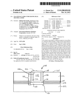
  • 1. c12) United States Patent Iwatake et al. (54) VIA CONTACT STRUCTURE HAVING DUAL SILICIDE LAYERS (75) Inventors: Michael M. Iwatake, Wappingers Falls, NY (US); Kevin E. Mello, Fishkill, NY (US); Matthew W. Oonk, Poughkeepsie, NY (US); Amanda L. Piper, Poughkeepsie, NY (US); Yun Y. Wang, Poughquag, NY (US); Keith K. Wong, Wappingers Falls, NY (US) (73) Assignee: International Business Machines Corporation, Armonk, NY (US) ( *) Notice: Subject to any disclaimer, the term ofthis patent is extended or adjusted under 35 U.S.C. 154(b) by 2197 days. (21) Appl. No.: 10/711,298 (22) Filed: Sep.9,2004 (65) Prior Publication Data US 2006/0051959 Al Mar. 9, 2006 (51) Int. Cl. HOJL 23152 (2006.01) (52) U.S. Cl. ........ 257/384; 257/389; 257/751; 257/757; 257/E29.268 (58) Field of Classification Search .......... 257/750-754, 257/763-764,768-770,384,389, 757,E29.268 See application file for complete search history. 111111 1111111111111111111111111111111111111111111111111111111111111 US008288828B2 (10) Patent No.: US 8,288,828 B2 Oct. 16, 2012(45) Date of Patent: (56) References Cited U.S. PATENT DOCUMENTS 5,094,981 A * 5,565,708 A * 5,571,753 A * 5,834,846 A 6,277,729 B1 * 6,613,670 B2 * 6,677,230 B2 3/1992 Chung eta!. .................. 438/621 10/1996 Ohsaki eta!. ................. 257/764 1111996 Saruwatari .................... 438/527 1111998 Shinriki eta!. 8/2001 Wu et a!. ....................... 438/627 9/2003 Rha eta!. ...................... 438/657 112004 Yokoyama eta!. 2002/0019127 A1 212002 Givens FOREIGN PATENT DOCUMENTS JP 08-107087 * 4/1996 * cited by examiner Primary Examiner- Anh Mai (74) Attorney, Agent, or Firm- Yuanmin Cai (57) ABSTRACT A via contact is provided to a diffusion region at a top surface ofa substrate which includes a single-crystal semiconductor region. The via contact includes a first layer which consists essentially of a silicide of a first metal in contact with the diffusionregion at the top surface. A dielectric region overlies the first layer, the dielectric region having an outer surface and an opening extending from the outer surface to the top surface ofthe substrate. A second layer lines the opening and contacts the top surface of the substrate in the opening, the second layer including a second metal which lines a sidewall of the opening and a silicide of the second metal which is self- aligned to the top surface of the substrate in the opening. A diffusion barrier layer overlies the second layer within the opening. A third layer including a third metal overlies the diffusion barrier layer and fills the opening. 10 Claims, 3 Drawing Sheets JOO 1'1-t. !lo ~·~ I'~ ~~!If> /tz.O ~..... '/~ r- _21_ lo~"-..( / f.- IL-'2- L2::- ' (1 os / yiOfo 1/llh / - '.. 0 ------ / ,.- ..._.l { ----.,.,. o6 03 r---{02
  • 2. U.S. Patent Oct. 16, 2012 Sheet 1 of 3 JOO ltb ll ~~1 f~~ 0 . --..,.,. ,-- liZ ~ / lol{0 -- 12Y j00 / / -I '2"2.. /!lh / " ~ l1os ~ ' 0 FIG. 2 / lol f ) <......./ FIG. 3 ) US 8,288,828 B2 /120 ,...-- .,. 1'---l I ~ oG 103 ,-~ 102 . - lrP 03~ -I ..-- _, ---- '- lo5 --- ~ lo'2
  • 3. U.S. Patent Oct. 16, 2012 Sheet 2 of 3 FIG. 4 ?lO jJD-. ~~32.. ~tot FIG. 5 .~ ,10 I 11J)-__ ~.--1c~ !32-- ~ .J,. -.. 1,atrL,?}i FIG. 6 ITZ.~ t'- )-/Db ~/ / 1' '10 US 8,288,828 B2 -- ... ... 'CS 103 -··I- (02.. ~I- 11'2.. .-{02
  • 4. U.S. Patent Oct. 16, 2012 Sheet 3 of 3 US 8,288,828 B2 FIG. 7 /r-JJD / I 11~ 120 ,.. ~ -11-1..- ~ ,~lo0 FIG. 8 /. to?! .0
  • 5. US 8,288,828 B2 1 VIA CONTACT STRUCTURE HAVING DUAL SILICIDE LAYERS BACKGROUND OF INVENTION The present invention relates to integrated circuits and their fabrication. More specifically, the invention relates to the structure and fabrication ofa via contact to a diffusion region at a top surface ofa single-crystal semiconductor region ofa substrate. A particular challenge encountered in the fabrication of integrated circuits is the formation ofmetallic via contacts to diffusion regions (referred to alternatively as "diffusions") of semiconductor devices. Such diffusion regions are formed in single-crystal semiconductor regions ofa substrate, such that an ohmic contact is made between the metallic material in the via and the semiconductor material of the diffusion region. The challenge is particularly difficult to provide a robust structure and method offorming metallic via contacts having acceptably low contact resistance between the metal and the diffusion region, over all chip locations of an entire wafer. Thus, processes and structures known heretofore have resulted in acceptable contact resistance, but only when a sufficiently thick layer of a metal silicide, e.g., greater than 20-25 nm of cobalt silicide (CoSi2 ) or nickel monosilicide (NiSi), for example, is provided at a top surface ofthe diffu- sion region. In one such exemplary process, a metal silicide layer is formed in contact with the diffusion region of the substrate, after which an interlevel dielectric (ILD) is formed, typically consisting essentially ofa highly flowable, planariz- ing dielectric such as borophosphosilicate glass (BPSG), undoped silicate glass (USG) or silicon dioxide deposited from a tetraethylorthosilicate (TEOS) precursor. Thereafter, the ILD is patternedto form an opening overthe metal suicide layer. A sputter clean process is then performed to clean the surface ofthe pre-existing metal silicide layer to make it ready for the deposition of metallic layers which enhance the conductive contact and to prepare the via to be filled with tungsten by a chemical vapor deposition (CVD) technique. However, the sputter clean process consumes some ofthe pre-existing metal silicide layer at the top surface ofthe single-crystal semiconductor region. In an example, the sputter clean process removes about 8 nm of the metal sili- cide. Thereafter, a thin layer of a metal such as titanium (Ti) 2 throughput and cost of each wafer. In addition, a thicker Ti layer is undesirable because the sputtering process tends to deposit more Ti at the entrance (top) surface of a via, while depositing comparatively less Ti at the bottom of the via. Accordingly, a byproduct of the Ti sputter deposition is a more constricted opening, sometimes having a re-entrant pro- file, that is more difficult to fill in subsequent depositions to form the TiN diffusion barrier layer and theW metal fill. Ifthe Ti layer is not kept to the minimum thickness, theW fill metal 10 deposition must be more tightly controlled to prevent voids and pinch-offofthe via opening from occurring during depo- sition. Still another reason limiting the thickness of the Ti layer is a goal of the conventional process to intentionally 15 limit the amount of Ti present in the via. The conventional process intentionally limits the amount of Ti in the via as a way of limiting damage, in case the TiN diffusion barrier layer fails in some areas ofthe wafer during tungsten CVD. If the TiN layer fails as a barrier, this allows the Ti to interact 20 with the WF6 precursor gas. However, WF6 produces volatile compounds when it comes into contact with portions ofthe Ti layer. Suchvolatile compounds destructively impact the prior deposited layers, the W layer during deposition and subse- quently deposited layers, causing severe degradation of the 25 via structure and degrading its performance. Thus, in the conventional process, the Ti layer is kept intentionally thin for a variety ofreasons, all ofwhich are intended to improve the quality of the contact structure. However, the above-described process only produces 30 acceptable results when the pre-existing silicide layer under- lying the ILD, i.e., the CoSi2 or NiSi layer, is relatively thick, i.e., having a thickness in excess of 20 nm to 25 nm. That thickness is needed in order for the silicide layer under the ILD to remain to a sufficient thickness at locations all overthe 35 wafer after the openings in the ILD are subjected to the above-described sputter clean process. Ifa smaller thickness ofthe silicide were used, e.g., having a nominal thickness of 10 to 12 nm, the sputter clean process could result in remov- ing the silicide layer entirely in some locations ofthe wafer. In 40 such case, poor contact to the diffusion region of the semi- conductor material would result, having poor contact resis- tance. This is a problem that needs to be addressed. SUMMARY OF INVENTION is sputter deposited inside the via opening. For example, a 45 layer of titanium having a thickness of 20 angstroms (A) or less is deposited at the bottom of the opening, the deposited titanium being, illustratively, about 100 A thick where it overlies the ILD in the field. The Ti layer promotes adhesion According to an aspect of the invention, a via contact in a via contact structure is provided to a diffusion region at a top surface of a substrate which includes a single-crystal semi- conductor region. The via contact structure includes a first layer which consists essentially ofa silicide ofa first metal in contact with the diffusion region at the top surface. A dielec- tric region overlies the first layer, the dielectric region having an outer surface and an opening extending from the outer surface to the top surface ofthe substrate. A second layer lines the opening and contacts the top surface ofthe substrate in the opening, the second layer including a second metal which lines a sidewall of the opening and a silicide of the second metal which is self-aligned to the top surface ofthe substrate in the opening. A diffusion barrier layer overlies the second layer within the opening. A third layer including a third metal overlies the diffusion barrier layer and tills the opening. to the bottom and sidewalls ofthe opening. The Ti layer is also 50 used to getter oxygen from a native oxide that forms on the surface of the pre-existing metal silicide layer. The Ti layer used in the conventional process is deposited to a thickness of 20 A or less because such thickness is sufficient to promote desired adhesion properties and to perform oxygen gettering 55 from the underlying metal silicide layer. Thereafter, a diffusion barrier layer suchas titanium nitride (TiN) is CVD deposited onto the underlying Ti layer, as a barrierto the diffusion and electromigrationofmaterial to and from the underlying Ti and silicide layers and materials 60 present during subsequent depositions. Thereafter, a metal such as W (tungsten) is deposited, such as by CVD from a tungsten hexaflouride (WF6 ) precursor, to fill the via after forming the Ti and TiN layers. In the conventional process, a Ti layer having a thickness 65 greater than 20 A is undesirable because the sputter deposi- tion of titanium takes up significant time, impacting the BRIEF DESCRIPTION OF DRAWINGS FIG.l is a cross-sectional view illustrating a completed via contact structure according to an embodiment of the inven- tion.
  • 6. US 8,288,828 B2 3 FIGS. 2 through 8 further illustrate stages in a method of fabricating a contact via according to an embodiment of the invention. DETAILED DESCRIPTION It is common for transistors which have silicided diffusion regions to be contactedthrough openings formed in dielectric regions which overlie the diffusion regions, such as described in the foregoing. However, the demands ofcurrent and future generation transistors are not adequately served by tradition- ally thick suicides which underlie the ILD at the top surface of the diffusion region. 4 200 nm, and most preferably having a width between about 100 nm and 150 nm. The opening has height extending from the outer surface 120 of the ILD 112 to the diffusion region 102 ofbetween about 150 nm and about 600 nm, more pref- erably between about 200 nm and 500 nm, and most prefer- ably between about 200 nm and 300 nm. The opening 110 and via contact 100 therein are disposed in the ILD 112 overlying a first layer 103 including a silicide ofa first metal, the silicide being disposed in contact with the top surface 101 of the 10 diffusion region 102. The first layer 103 preferably has a thickness of between about 8 nm and 15 nm, and more pref- erably between about 10 nm and 13 nm. Such thickness is much smallerthan the thickness ofgreaterthan 20to 25 nm of For a variety ofreasons, it would be desirable to make the silicide thinner that underlies the ILD at the top surface ofthe 15 diffusion region. For one, a thinner silicide helps to reduce leakage current of devices that are formed in bulk semicon- ductor substrates. A thinner silicide also promotes a better contact to the diffusion regions ofdevices that are formed in CoSi2 or NiSi that is used in the above-described prior art process. A layer 105 of an etch-distinguishable material is further disposed between the first layer 103 and the ILD 112. That layer 105 functions as an etch stop layer when the opening 110 is etched in the ILD 112, to stop the etching process from proceeding to etch the diffusion region 102 after the etched opening penetrates the ILD 112. A suitable material for the a thin semiconductor-on-insulator layer or a silicon-on-insu- 20 lator layer, both referred to hereinafter as an "SOl" layer. A third reason why a thinner suicide underlying the ILD would etch stop layer 105 is silicon nitride, when the ILD 112 includes an oxide such as the various forms ofsilicon oxides, e.g., BPSG, USG, or a TEOS oxide, that are typically used for that purpose, as discussed above in the background. Alterna- tively, the etch stop layer 105 can consist essentially of any be advantageous is to help better control the position of the edge ofthe silicide relative to the channel region ofa transis- tor, when the transistor has a small channel width. This con- 25 siderationis especially important when spacers separating the gate of the transistor from the source and drain diffusions thereof are smaller than desirable. In such case, a thinner silicide would help to produce better small channel width transistors, even when the spacer thickness is smaller than 30 that considered acceptable for transistors having a traditional thicker silicide. material to which etch selectivity can be achieved when etch- ing the overlying ILD 112. The thickness of the etch stop layer 105 is illustratively between about 2 nm and 30 nm, more preferably between about 5 nm and 15 nm, and most preferably about 7 to 10 nm. The via contact 100 includes a second layer 104 ofmaterial According to the embodiments ofthe invention, a process is provided herein which allows a contact having acceptable contact resistance to be made to the surface of a silicided 35 contacting a top surface 101 of the diffusion region 102, the second layer 104 including a layer 106 consisting essentially ofa second metal lining the sidewalls ofthe opening 110, and also including a silicide 108 of the second metal that is dis-diffusion region, even when a thinner silicide is provided on the surface of the diffusion region underlying an interlevel dielectric (ILD). According to the embodiments ofthe inven- tion, a via contact is provided in which a metal-containing layer is formed in an opening in a dielectric layer above the silicided diffusion region, that layer contacting the top sur- face of the diffusion region in the opening. Such layer includes a metal lining the sidewall of the opening, and a silicide of that metal self-aligned to the top surface of the diffusion region in the opening. A diffusion barrier layer overlies that metal-containing layer in the opening, and a further layer ofmetal fills the opening overlying the diffusion barrier layer. A cross-sectional view of a completed via contact 100 according to the invention is illustrated in FIG. 1. As shown therein, the via contact extends to a top surface 101 of a diffusion region 102 ofa single-crystal semiconductor region of a substrate. Illustratively, the substrate is a bulk semicon- ductor substrate or a semiconductor-on-insulator (SOl) sub- strate such as a silicon-on-insulator substrate. In preferred embodiments of the invention, the single-crystal semicon- ductor region consists essentially of silicon. However, other semiconductor materials can be utilized such as alloys of silicon, e.g., silicon germanium and silicon carbide. Alterna- tively, III-V compound semiconductors and/or II-VI com- pound semiconductors are usable in other embodiments of the invention. The via contact 100 is disposed in an opening 110 in a dielectric region 112, preferably an interlevel dielectric (ILD), overlying a top surface 101 ofthe diffusion region 102 ofthe substrate. The opening has width ofbetween about 50 nm and 400 nm, more preferably between about 100 nm to posed in contact with the top surface 101 of the diffusion region 102. Preferably, the layer 106 consists essentially ofa silicide-forming metal such as titanium (Ti), cobalt (Co), 40 nickel (Ni), tantalum (Ta), platinum (Pt), tungsten (W) or combination thereof, and layer 108 includes the silicide of that metal. Thus, when the diffusion region 102 is disposed in single-crystal silicon, examples of a material included in the silicide layer 108 include, but are not limited to: TiSix, CoSix, 45 TiCoSix, NiSi, NiCoSix, TaSi2 , PtSi2 , and WSix. When the diffusionregion 102 is disposed in silicon germanium (SiGe), the silicide layer 108 can include materials such as one or more of the suicides including, but not limited to: TiSixGeY, CoSixGey, TiCoSixGey, NiSixGey, NiCoSixGey, TaSixGey, 50 PtSixGey, and WSixGey The layer 106 of metal lining the sidewall 114 of the opening 110 can either have uniform thickness, or instead be subject to variations in thickness from a lower edge 116 to an upper edge 118 ofthe layer 106. When depositing metal into 55 an opening, variations in the thickness of deposited material are subject to occur based on proximity of the surface to the source of material to be deposited. Hence, parts ofthe open- ing 110 in the ILD 112 which are closer to the outer surface 120 thereofare more likely to receive a thicker layer ofmetal 60 during a deposition ofthe metal layer into the opening, while parts ofthe opening 110 that are closer to the surface 101 of the diffusion region 102 of the substrate are more likely to receive a thinner layer of metal during the deposition. The embodiments of the invention described herein are suitable 65 for use regardless of the thickness of the deposited metal in different parts ofthe opening 110 inwhich the via contact 100 is disposed.
  • 7. US 8,288,828 B2 5 6 As further shown in FIG. 1, the via contact further includes a diffusion barrier layer 122 overlying the secondlayer 104.A further layer 124 overlies the diffusion barrier layer 122, that layer 124 including a third metal which fills the remaining opening 110, preferably to the level ofthe outer surface 120 of 5 the ILD 112. The diffusion barrier layer 122 preferably includes a conductive nitride material. Metal nitrides such as titanium nitride (TiN), tantalum nitride (TaN), tungsten nitride (WNx) and nitrides of vanadium (V), niobium (Nb), hafnium (Hf) and zirconium (Zr) are suitable for this purpose. 10 Preferably, the metal nitride includes a nitride of the second metal that is included in the second layer 106. Thus, when the second metal is Ti, or Ta, the conductive nitride is a nitride of that second metal, i.e., either TiN, or TaN, respectively. When the diffusion barrier layer 122 includes TiN, it preferably has 15 a thickness of between about 3 nm and 10 nm, and more preferably about 5 nm. preferably formed by a low temperature deposition of a highly flowable, planarizing oxide such as borophosphosili- cate glass (BPSG), or, alternatively, from a tetraethylortho- silicate (TEOS) precursor. In other alternatives, a spin-on- glass (SOG) material having planarizing qualities is flowed onto a wafer containing the structure shown in FIG. 3, and thereafter, the wafer is rotated to distribute the SOG material to a more or less uniform height above the top surface 101 of the diffusion region 102, followed by baking to density the distributed SOG layer. In still another alternative, a denser oxide such as one deposited by a high-density plasma (HDP) technique is deposited onto the structure and, thereafter, pla- narized by additional processing such as chemical mechani- cal polishing (CMP). FIG. 4 illustrates a subsequent stage in which an opening is formed in eachofthe ILD 112, the etch stop layer 105, andthe first layer 103. Preferably, the opening in the ILD 112 is formed by an anisotropic etch such as a reactive ion etch (RIE), performed selectively to the material of the etch stop layer 105. For example, when the etch stop layer contains a nitride, the RIE process is conducted selective to that nitride. The via contact 100 further includes a filler metal 124 disposed in the opening 110 ofthe ILD 112. Ideally, the filler metal 124 is formed in such way that no void results in the 20 opening 110. Voids are detrimental to the long-term reliability ofthe via contact 100, as well as those structures to which the via contact is juxtaposed, i.e., the diffusion region 102. Examples of metals for use as the filler metal 124 include tungsten, and aluminum which can be deposited by efficient 25 techniques that result in good filling qualities, such as by chemical vapor deposition (CVD). Tungsten is the preferred metal for a variety of reasons, as will be described further below. This causes etching to stop on the etch stop layer 105. With sufficient selectivity, an over-etch can be performed to ensure that all such openings on a wafer are fully etchedto expose the etch stop layer 105, thus assuring that the etched openings reach the intended level of the structure underlying the ILD 112. Thereafter, the etch stop layer 103 is preferably cleared from the opening, as by isotropically etching selective to the underlying silicide material of the first layer 103, and the As further shown in FIG. 1, the top surface 126 of the via contact 100 preferably presents a planar surface, i.e., pla- narized to the outer surface 120 ofthe ILD 112, for allowing good contact to be made thereto from higher level metalliza- tions (not shown) that are provided subsequently thereto. FIGS. 2 through 8 illustrate a method of fabricating a contact via according to an embodiment of the invention. FIG. 2 illustrates a preliminary stage in the fabrication. As shown therein, a first layer 103 containing a silicide ofa first metal is disposed at a top surface 101 ofa diffusionregion 102 ofa single-crystal semiconductor region ofa substrate. Prior to forming the first layer 103, a dopant implant is preferably performed to increase the concentration of dopant ions near the top surface 101, thereby enhancing the conductivity ofthe diffusionregion 102 at the surface 101. The silicide ofthe first layer 103 is formed preferably by a self-aligned technique in which a silicide precursor metal is deposited in contact with the top surface 101 of the diffusion region 102, that region preferably being formed in a single-crystal silicon region or silicon alloy region (e.g., SiGe region) ofa substrate and then reacted by annealing to form the silicide. Examples of suit- able silicide precursor metals include, but are not limited to: cobalt, nickel, molybdenum, niobium, palladium, platinum, tantalum, titanium, vanadium and tungsten. Alternatively, the first layer 103 is formed by deposition of a silicide onto the single-crystal semiconductor region 102 in an additive or subtractive patterning process. The first layer is preferably formed having a nominal thickness between about 8 nm and 15 nm, and more preferably having a nominal thickness between about 10 nm and 13 nm. Generally, it is not possible to maintain the thickness of the first layer uniform across an entire wafer. Therefore, when the first layer is deposited to a thickness of 10 nm in some places ofthe wafer, the thickness can be significantly lower in other places ofthe wafer. Thus, a thickness of 8 nm or lower may result in some areas of the wafer. Thereafter, as shown in FIG. 3, the interlevel dielectric (ILD) 112 is formed over the etch stop layer 105. The ILD is 30 material of the ILD 112. In a further etch step, a sputter "clean"process is performed in the opening 110 using a beam ofparticles to remove residues from prior etching that remain on the sidewall130 and bottom 132 ofthe opening 110. In a preferred process, this sputter etch step removes the upper- 35 most 8 nm of material from the bottom 132 of the opening 110. Thus, this step removes a significant portion of the first layer 103 of silicide that is provided on the diffusion region. In fact, sputter clean processes generally have some non- uniformity across a wafer, such that a greater thickness of 40 material is removed in some areas than others. Moreover, as discussed above, the thickness ofthe first layer 103 ofsilicide is subject to vary across the wafer. Accordingly, at least in some areas of the wafer, the sputter clean process results in the entire removal of the first layer 103 within the opening 45 110, thus exposing the top surface 101 ofthe diffusion region 102 in the opening. Thereafter, as shown in FIG. 5, a second layer 106 includ- ing a second metal is deposited to line the bottom 132 and sidewalls 130 ofthe opening 110. The deposited second metal 50 is capable offorming a silicide with the exposed silicon at the top surface 101 of the diffusion region 102. The deposited second metal also promotes adhesion between the sidewall 130 ofthe dielectric region 112 and one ormore materials that are deposited subsequently within the opening. The second 55 metal preferably consists essentially of one or more of the metals: titanium (Ti), cobalt (Co), nickel (Ni), tantalum (Ta), platinum (Pt) or tungsten (W) and is preferably deposited into the opening by sputtering. More preferably, the second metal consists essentially of Ti. When the second metal consists 60 essentially ofTi, it is preferably deposited to a nominal thick- ness ofat least 30 angstroms (A) at a point ofcontact with the top surface 101 of the diffusion region 102. Variations in the characterofthe sputtering process across the wafermay cause the actual thickness 134 ofthe deposited second metal at the 65 top surface 101 to be somewhat greater or less than the nomi- nal thickness. More preferably, the Ti is deposited to a nomi- nal thickness ofbetween 40 Aand 80 Ain contact with the top
  • 8. US 8,288,828 B2 7 surface 101 of the diffusion region. Moreover, the deposited thickness ofthe layer is typically greater in areas ofthe wafer which are closer to the source ofthe sputtered species. There- fore, a deposited thickness 134 of40 to 50 Aat the top surface 101 of the diffusion region corresponds to a nominal depos- ited thickness 136 of30 nm overlying the outer surface 120 of the ILD 112. A somewhat greater deposited thickness 134 of 8 contact via 100 to higher level interconnect structures on an integrated circuit or other device in which the contact via is disposed. As indicated above, the embodiments of the invention described herein provide a contact via having acceptable con- tact resistance, despite that the initial silicide layer 103 is removed during the initial formation of the opening. Mea- surements performed on contact vias processed according to the above-described embodiments indicate acceptable con- 60 to 80 A at the top surface 101 corresponds to a nominal deposited thickness 136 of40 nm overlying the outer surface 120 ofthe ILD 112. Here, the thickness ofthe second layer at the top surface 101 is being controlled according to the embodiments of the invention. Thereafter, as shown in FIG. 6, a diffusionbarrierlayer 122 10 tact resistance when the second layer is deposited to a nomi- nal thickness 136 (FIG. 5), as measured above the outer surface 120 ofthe dielectric region, of30 nm or more, while a deposited thickness of 20 nm and less shows poor contact resistance. The measurements are indicated below.is formed overlying the second metal layer 106. The diffusion barrier layer 122 preferably includes a conductive nitride 15 material. Preferably, when the second metal is Ti, the conduc- tive nitride consists essentially ofTiN, as being a nitride ofthe second metal that is included in the second layer 106. Other metal nitrides such as tantalum nitride (TaN), tungsten nitride (WNx) and nitrides of V, Nb, Hf and Zr are also suitable. 20 Preferably, the conductive nitride material, such as TiN, is deposited by CVD, because CVD produces a TiN layer hav- ing more uniform coverage than a TiN layer deposited by sputtering. In addition, a TiN layer can be deposited in a shorter amount oftime by CVD than such layer can be depos- 25 ited by sputtering. As shown in FIG. 7, a further layer 124 is then deposited to overlie the diffusion barrier layer 122, that layer 124 including a third metal which fills the remaining opening 110. The third metal 124 is deposited to fill the opening 110 and extend onto the region above the outer 30 surface 120 of the ILD 112. Preferably, the third metal is depositedby any ofseveral well-known chemical vapor depo- sition (CVD) processes such as ordinary CVD, plasma enhanced CVD (PECVD), metalorganic (MOCVD), or low- pressure CVD (LPCVD). Ideally, the filler metal 124 is 35 deposited in such way to prevent voids from forming within the opening 110. Examples ofmetals for use as the filler metal 124 include tungsten (W) and aluminum (AI) both of which can be deposited by one or more ofthe above-indicated tech- niques to produce good fill characteristics. Tungsten is a 40 preferred metal because it can be deposited by well-under- stood CVD techniques over an underlying diffusion barrier layer ofTiN. Thereafter, after the above-described processes have been performed, annealing is performed to react the second metal 45 at the top surface 101 with the silicon present at the top surface 101 to produce a silicide 108, as shown in FIG. 8. This silicide forms an ohmic contact to the diffusion region. Depending upon the specific metal or metals that are depos- ited as the second layer 106, the silicide layer 108 includes, 50 but is not limited to any one or more ofthe suicides ofcobalt (Co), nickel (Ni), platinum (Pt), tantalum (Ta), titanium (Ti), and tungsten (W). Preferably, the silicide layer includes one or more ofTiSix, CoSix, TiCoSix, NiSi, NiCoSix, TaSi2 , PtSi2 , and WSix. When the diffusion region 102 is disposed in sili- 55 con germanium (SiGe), the silicide layer 108 can include, but is not limited to any one or more of the suicides and ger- manides of cobalt (Co), nickel (Ni), platinum (Pt), tantalum (Ta), titanium (Ti), and tungsten (W), and especially: TiSixGey, CoSixGey, TiCoSixGey, NiSixGey, NiCoSixGey, 60 TaSixGey, PtSixGey, and WSixGey- Referring to FIG. 1 again, thereafter, the top surface 126 of the conductive filler material 124 is planarized to the outer surface 120 of the dielectric region, such as by a chemical mechanical polishing (CMP) or other suitable known pia- 65 narization technique. Thereafter, additional contact struc- tures and processing, can be used to further interconnect the Thickness 136 (FIG. 5) 20 nrn 30 nrn 40nrn Average Resistance per Contact 23 ohm 13 ohm 13 ohm While the invention has been described in accordance with certain preferred embodiments thereof, those skilled in the art will understand the many modifications and enhancements which can be made thereto without departing from the true scope and spirit ofthe invention, which is limited only by the claims appended below. What is claimed is: 1. A via contact structure having a via contact to a diffusion region at a top surface ofa substrate, the via contact structure comprising: a first layer consisting essentially of a silicide of a first metal in contact with said diffusion region at said top surface; a dielectric region overlying said first layer, said dielectric region having an outer surface and an opening extending from said outer surface through saidfirst layerto saidtop surface of said substrate; a second layer lining said opening and contacting said top surface in said opening, said second layer including a second metal lining a sidewall of said opening and a silicide of said second metal self-aligned to said top surface in said opening; a diffusion barrier layer overlying said second layer within said opening; and a third layer including a third metal overlying said diffu- sion barrier layer and filling said opening. 2. The via contact structure as claimed in claim 1, wherein said first metal is selected from the group consisting ofcobalt (Co), molybdenum (Mo), niobium (Nb), nickel (Ni), palla- dium (Pd), platinum (Pt), tantalum (Ta), titanium (Ti), vana- dium (V) and tungsten (W). 3. The via contact structure as claimed in claim 2, wherein said second metal is selected from the group consisting of titanium (Ti), nickel (Ni), platinum (Pt), cobalt (Co), tantalum (Ta), and tungsten (W). 4. The via contact structure as claimed in claim 3, wherein said first metal and said second metal are the same. 5. The via contact structure as claimed in claim 3, wherein said first metal consists essentially ofcobalt and said second metal consists essentially of titanium. 6. The via contact structure as claimed in claim 1 wherein said diffusion barrier layer includes a metal nitride. 7. The via contact structure as claimed in claim 6, wherein said metal nitride includes titanium nitride (TiN).
  • 9. US 8,288,828 B2 9 8. The via contact structure as claimed in claim 1, wherein said third metal includes tungsten (W). 9. The via contact structure as claimed in claim 1, wherein said opening has a width of about 250 nm or less and a height-to-width aspect ratio greater than one. 10 10. The via contact structure as claimed in claim 9, wherein said aspect ratio value is about two. * * * * *