SlideShare uma empresa Scribd logo
1 de 60
Baixar para ler offline
SM-1645 SERIES
SYNTHESIZED
MOBILE RADIOS
January 1987
CONTENTS
Specifications .............................................................. I
Location of Controls ........................................................ 2
Operating Procedure........................................................ 2
.......................................................EPROM Programming 3
Circuit Descriptions......................................................... 5
Parts Variation vs. Frequency Chart ...........................................12
Alignment and Adjustment ..................................................14
Troubleshooting............................................................17
Suggested Test Equipment...................................................17
Block Diagrams ............................................................18
PC Board Layouts and Schematics.............................................22
Parts List ..................................................................48
Warranty.................................................................. 55
SM-1645 Series
Mobilesand MobileRepeater
This Equipment Meetsor Exceeds the FollowingSpecifications
General SM-1645H SM-1645L SM-1645HS
Transmitter
Weight
144- 174 MHz
16
12 MHz
- 30 to +60C
13.8 VDC
9.1 amps
.98 amps
50 ohms
5 PPM
Dual EPROMS
5 or 12.5 KHz
11.7 x 7.2 x 2.6 inches
Frequency Range
Channels
FrequencySpread
Operating Temperature
OperatingVoltage
Current Drain(TX)
Current Drain(RX)
Antenna Impedance
FrequencyStability
Programming
Channel Spacing
Size
4 Ibs. 2 02s.

Specifications subject to change without notice.
136- 174 MHz
16
12 MHz
- 30 to +60C
13.8 W C
8.5 amps
.8amps
50 ohms
5 PPM
EPROM
5 or 12.5 KHz
7.2 x 2.6 x 10 inches
RF Output Power
Modulation
Spuriousand Harmonics
Hum and Noise
Audio Distortion
30 - 50 MHz
16
2.5 MHz
- 30 to +60C
13.8 VDC
9.0 amps
.8amps
50 ohms
5 PPM
EPROM
5 or 12.5 KHz
7.2 x 2.6 x 10 inches
4 Ibs.2 02s.
45 Watts (adj. 10-50)
16-
- 80 dB
- 50 dB
3%
45 Watts (adj. 10- 50)
16-
- 80 dB
-50 dB
3%
.25 u V ( 12 dB SINADJ
-85 dB
- 85 dB
- 75 dB
- 50 dB
5 Watts
5 Ibs 4 02s.
35 (adj.)
16B
- 80 dB
- 50 dB
3%
.25 uV ( 12 dB SINAD)
- 85 dB
- 85 dB
- 75 dB
- 50 dB
5 Watts
Sensitivity
Selectivity
Imageand Spurious
IntermodulationRejection
Hum and Noise
Audio Output
.25 UV(12 dB SINAD)
- 85 dB
-85 dB
- 75 dB
- 50 dB
5 Watts
LOCATIONOFCONTROLS
"Transmit" Indicator "Busy" lndlcator
1 pOwerswitchonloff~
Squelch Control and
Scanned Channels Designator
Microphone Receptacle (with Scan Option) Channel Select
OPERATING PROCEDURE
1. Turn the "Volume Control" clockwise to apply 5. When the channel is clear (background noise
power. The channel indicator will illuminate. only), rotate the "Squelch Control" clockwise
2. Set the "Channel Select" switch to the desired until the receiver is silenced. Perform this step
channel, as shown in the "Channel Indicator" carefully. Donotgo far beyondthesilencingpoint
window. or the receiver may not respond to weak signals.
3. Rotate the "Squelch Control'' counterclockwise. 6. After setting the receiver controls and seleaing ,
4. Adjust the "Volume Control" for a normal theproperchannel, depressthe microphonepush
listening level (background noise or a station if tatalk switch and speak across the face of the
one is transmitting). microphone in a normal voice when transmitting. ,
PRIORITY SCAN INSTRUCTIONS
1. Turn the radio on. 6. Activate the scan mode bydepressingthe "Scan"
2. Selectthrough thechannelsandusethe "Delete/ switch. A t this time the channel display will
Add" switch (detent of squelch pot) to delete indicate scanning of the channels in the scan list
those channelsthat are to be skipped during the
scan sequence. As channels are deleted the tone 7. Verify the priority monitor by opening "Squelch"
light will extinguish. on a non-priority channel andnoticing the "look-
3. Set the "Squelch Control" to quiet the receiver. back" action to priority channel.
(Thisshould be set on a non-active channel.)
4. Set the "Channel Selector" to the channel that is 8. Reset the "Squelch" to threshold.
to be the priority channel.
5. Engage the priority monitor by depressing the 9. Removethe microphonefrom itS brackettoassure
"Prioriv' switch. (This step should only be priority channel switching.
included if the prioritychannel is to be monitored
at all times.) 10. Replace the microphone.
-2 -
General
Transmit and receive frequencies are determined
from binary informationstored in the EPROM, IC703.
If the MT-20 Multi Tone option is installed, CTCSS
Encode and Decode frequencies are also derived
from binary information stored in the same EPROM.
Datafcr eachchannelconsistsof 16 bytesor memory
locations. The first 8 bytes control receive frequency
and tone and the second block of 8 bytes control
transmit frequency and tone. Each byte or memory
locationstores8 bits of data. The upper four bits are
tone informationandthe lowerfour bitsarefrequem
cy information. If no CTCSS Encode or Decode is
programmed, then the upper four bits of each
memory location will remain all ones, or, as repre-
sented in Hex."F." The transmitor receivefrequency
data is strobed into the synthesizer in eight-four bit
blocks, via four data linesfrom the EPROM.Thisdata
sets the counters internal to the synthesizer so that
the appropriate VCO oscillates at the desired fre-
quency. The addresses of the data to be sent to the
synthesizer are obtained from the Channel Select
switch and the TX/RX mode input to the EPROM.
Computation of ROM Data:
Counter data can be determined mathematically
using the formulas shown below. The result of the
computations will consist of 8 figures in Hex format
for each transmit or receive frequency.
The following example for channel 1 is based on a
simplex frequency of 154.430 MHz without CTCSS.
Note that the receiveHexcode is computed for 21.6
MHz below the desired receive frequency. For l o w
band radios 2 1.6 MHz will be added to the receive
frequency instead of subtracted. The eight data
values for each transmit or receive frequencywill be
labeled DO thru D7 and shown in Hex.
RECEIVER DATA:
VCO freq: 154.430- 2 1.6 = 132.83 MHz
N= ( 132.830 x 1000j/ 5 =26566
(5 being the channel spacing)
26566 / 10240 = 2.5943359375 (*)
W = lnteger value of above
D4 = 2.
Multiply figures to the right of the decimal by 16.
.5943359375 x 16 = 9.509375 (*)
D3 = lnteger value of above
D3 = 9
Again multiply fractionary remainder by 16.
,509375 x 16 = 8.15
D2 = 8
Multiply fractionary remainder by2.5
.I50 x 2.5 = 0.375
Dl = 0
Multiply fractionary remainder by 16.
.375 x 16 = 6.0
DO=nearestwhole number(ifafraction) which in
this case is 6
DO=6
So far we havevalues for DO thru W. The values for
D5 thru D7 are determined by the channel spacing.
Spacing can be 5 kHz (most U.S. frequencies) or 6.25
kHz spacing (mostly European). This is determinedby
whether the frequency is divisible by 5 or 6.25.
For 5 kHz steps:
M = O D 6 = C D7=3
For 6.25 kHz steps:
DS=O D6=O D7=3
The completedata loadfor 154.430MHz(RXJthen is:
DO=6, D l =0, D2=8, D3=9, W = 2 , D5=0,
D6=C,C7=3or(6 0 8 9 2 0 C 3 )
TRANSMllTER DATA:
VCO freq: 154.430
N=f154.430x10001/5=30866 .
(5 beingthe channelspacing)
30866 / 10240 =3.0162109375 (*)
W = 3
.0162109375 x 16 = .259375 (*)
D3 = 0
.259375 x 16 =4.15
D2 =4
.15 x 2.5 = .375
D l = 0
.375x 16 =6.0
DO=6
As before, channelspacing being 5 kHz, then:
D5 = 0, D6 = C, D7 = 3
The completedata loadfor 154.430 MHzTX then is:
DO=6, D l =O, D2=4, D3=O, W=3, D5=0,
D6=C,D7=3or(6 0 4 0 3 0 C 3)
It must be rememberedthat in the hexadecimalsys-
tem, numbersbetween 10 and 15 arerepresentedby
the lettersA thru F.
Ifwe were to program 154.430 TX/RX into channel
1, thecompletedataloadfor the first 16addressesof
the EPROM would then be:
F 6 m F 8 W R , m F C R , f i F O F 4 K ) n , H > F C n
Note that the upper 4 bits of each byte at each
address will be filled with one's (F), as they are
unusedbythesynthesizer.Also, the RXdataisalways
entered first
EXAMPLE DATA CHART
EPROM ADDRESS DATA LOAD FUNCTION REMARKS
00 Do F6 qRX)=I54.430 MHz
01 Dl FO qVCO)=154.430-21.6
02 DZ F8 =132.830 MH7
03 D3 F9
04 W R CHI
05 D5 FO RX
06 D6 FC
07 D7 I3
DO F6 F(TX)= 154.430MHz
Dl FO F(VCO]= 154.430
D2 F4
D3 FO
w n CHI
D5 FO TX
FC
137 n
('1 The dwision of N by 10240 and subsequent multiplicationof the fractional panby 16 should be done by hand or computer with appropriate
accuracy as these numbers can sometimes extend 12 decimalplacesand must be carried rather than roundedoff so as to maintainaccuracy.
-3-
CIRCUIT DESCRIPTION
RECEIVER
General 1st Local Oscillator
The SM-1645's double superheterodyne design em- See "PLL/Frequency Generation".
phasizes high sensitivity, low noise leveland excellent
selectivity.The first IF frequenq is 21.5 MHz and the
2nd
second IF frequency is 455 kHz.
0105 isa crystal-controlled oscillatorat 21.145 MHz,
RFAmplifler
A low-noise, dual-gate FET(0101)amplifies low-level
signalsfrom the antenna terminal and feeds the next
stage (1st Mixer).RF coils L101-L105 affect the band-
width, filter incomingsignalsand preventundesirable
radiationof the 1st localoscillator frequency.
1st Mixer
This function, performedby 0102, serves to mix the
incoming signal and that of the 1st local oscillator,
resulting in the 1st IF of 21.6 MHz. This stage is im-
portant inachieving a high level of intermodulation
rejection.
with the frequency fine adjustedby CVIOI.This signal ,
is fed into the 2nd mixer (0106).
Squelch Control Circuit
In a noise squelch circuit, the internal noise of the
receiver decreases when a signal is present. When
there is no incoming signal, noise is picked up and
amplified by half of IC102 and part of IC103. It is
then rectifiedby 0107 and converted to a DC level.
The DC signal is fed to a Schmitt Trigger Circuir
(comprisedof the other parts of IC103),which stops
the amplification function of lClO2 (DC-Controlled
Attenuator).
When there is incomingsignal, and the internal noise
decreases, the Noise Detector(0107)losesits output
1st IFAmplifler
and pin 10 of IC103 goes high, enabling IC102.The
This circuit, consistingof 0104, amplifies the 21.6 MHz squelch point is controlled by the squelch potenri-
signal. ometer, which varies the gain of lClO2 at the DC
level.
2nd Mlxer Busy Llght
This function, performed by 0106, serves to mix the Where tone squelch systems are incorporated into
frequency of the 2nd local oscillator, and to convert the radio, it is necessary to check for other signals
21.6 MHz to the 2nd IFof 455 Khz. before transmitting. The busy light indicator serves
that purpose.
2nd IFAmplifier The busy light functions off the high or low DC level
This staqe, containedwithin IC101, amplifiesthe455
at pin 10of IC103via LEDdriver transistor 0108. d
KHz 2nd IF. Italso performsthe limiting function.
Regulated Power Supply
Audlo Detector To keep fluctuations in power source voltage from
This circ~it,consistingof IC101 and F103, recoversthe influencing the receiver characteristics, IC105 feeds
audio signal from the 2nd IF. regulated voltage to the primary circuits, including
oscillator, squelch, RFamplifier and IFamplifier.
AF Amplifler
IC104 amplifies the audio signal from the previous Switching Clrcult
stage to the power level needed to drive the loud Inthe TX mode, the receiversupplyvoltageis removed
speaker. by 0109-0110 and 0105-0106.
CIRCUIT DESCRlPTlON
TRANSMIITER
General
The oscillator uses a programmable Phase Locked
Loop(PLL).The resultantVCO frequency is the same
as the channel frequency on transmit and 21.6 MHz
below channelfrequency on receive.Inthe transmit
mode, the VCO output is modulated, amplifiedand
fed to the antenna.
PLL, Exciter Boards
The circuits that make up the transmitter are:
PLL
Transmitter Exciter
Modulator
Power Supply
PLL/Frequency Generation
Transmitter drive at the carrier frequency and the
receiver 1st local oscillator signal (21.6 MHz below
the desired receive frequency)are generatedrespec-
tively by independent VCOs 0203 and 0201. The
signalfrom transmit VCO 0203 is bufferedby0204
before being fed to the TX exciter and PLL buffer
0205. The output from receiveVCO 0201isbuffered
by 0202 before being fed to the receiver 1st mixer.
In the receive mode, 0201 output is also fed to the
PLL buffer 0205 via 0204.
The frequencyof the respectiveVCOs are controlled
bya DCvoltage derived by the PLLcircuitry.The DC
voltage results from a phase/frequency comparison
between the divided-down frequency from the ref-
erence oscillator controlled by4.8 MHz crystalX2Ol
and the divided-down output from the VCO. These
functions are performed by the dual-modulus syn-
thesizer lC202.
XTAL heaters R267 and R268 stabilize the tempera-
ture of the reference oscillator. The heating is con-
trolled by0214 and 0215, and is proportional to the
ambient temperature as sensed by the thermistor
TH201. The resultantVCO controlvoltage(andhence
frequency) is determined by the divide ratio of the
counters internal to IC202. The VCO voltage will
vary between 1.5 volts at the lowest frequency and
7.5 volts at the highest.This voltage is generated by
0206,0207 and 0208 based on phase data from
the synthesizer IC202. Digital data, which sets the
internal counters (or divide-by ratios) i n ICZOZ, is
stored in an Erasable Programmable Read-Only
Memory(EPROM)IC203.
The synthesizer, IC202, requires32 bitsfor frequency
determination.Data is transferredor "strobed" into
IC202 in eight 4-bit "words" in order to simplify
interconnectionand package size. Strobing is done
byclockingthe addresses to the EPROMand IC202.
The data entering lUO2 via data pins DO-D3 isstored
in internal latches as determined by the address
present.
Address strobing is accomplished by clock IC205,
which drivescounter lC204. IC204converts theserial
clock pulses from IC205 to 3-line binary addresses
between 0 and 7 (decimal)at outputs 00-02.
PLLunlock protection is providedby0212 and 0213.
This circuit will disable the TX exciter in the absence
of lock detect at IC202.A high or "1" is supplied to
EPROM IC203 address line 3 (pin 5) during TX in
order to switch strobing up by eight addresses. This
allowsreceivedata to bestoredinthe first8 addresses
and transmit data within the next8 addressesof any
given 16 address "channel block" selected by the
channel select circuitry. Channel select addressing
takes place at address linesA4-A7 of the EPROM.
It is conceivable that up to eight 16-channel blocks
could be addressed via unused lines A8-A10 for a
total of 128 channels.
(The 2716 EPROM stores up to 2048 bytes. Each
channel requires 16 bytes, which provides room for
128 16-byte "groups".)
lC2Ol isadual moduluscounter controlledby IC202.
The dual modulus method simplifies overall design
byproviding a selecteddivision ratio on the input of
IC202.
Operating frequency versus VCO voltage is deter-
mined by Varicaps D2OI-D2O2 at the receive VCO
and D203-D204 at the transmit VCO. Modulation
of the transmit VCO is determined by applying the
audio signal to Varicap D205.
Transmitter Exciter
0209, 0 210 and 0 211 amplify the transmitter VCO
signalto asuitableinput levelfor thedriverstage(0.5W).
The stages are broadband transformer coupled and do
not require tuning.
Modulator
This stageconsistsof DualOp-Amp IC207.Onehalfacts
halfasaspeechamplifierandtheother halfprovidespre-
emphasisandlimiting.Appropriatehighfrequencyrolloff
is accomplishedbya low-passfilter on the output of the
secondstage.Microphonesensitivityisset byVR2O1 and
deviation by VR202.
Power Circuits
TX/RX switching is accomplishedb y 0 217and0 216.In
thereceivemode, 0 217saturatesasaresultofbasedrive
from 8 V regular IC206. Saturation of 0 217 providesa
ground path for RX VCO 0 2 01, thereby enabling it.
Shortening the PlT line to ground shunts base drive to
0 217, w5ich prevents it from conducting.This, in turn,
disables RX VCO 0 2 0I . In this condition, base current
flows through 0 216, causing it to saturate and to pro-
vide +8 V DCtothemodulator, TXVCO andRFpredriver
0209 via 0213, which is part of the lock detection
circuit.
Voltage regulation is providedby IC208 (+5 V DC for
the logic) and IC206 (+8 V DC for modulator and
TX v c o j .
DisplayBoard
A 7-segment 2digit LED is used to display the channel
beingused.FouradditionalLEDsserveto indicatevarious
functions of the radio.
The channel select switch sends out positive logic 4-bit
binarycodesrepresenting0 to 15 decimal.To convertthis
to 1 to 16, "1" is addedto the 4-bit code output by4-bit
parallel full adder lC6O1.
IC602convertsthe 5-bit binarycodefrom the adder to
2-digit BCD for the display. The upper digits are 0 to 1,
with 1 indicatingCh. 10toCh. 16.The 1-bit outputofthe
upperdigits isconnectedto 0 6 01, which drives theseg-
ment that corresponds to "1 " on the first digit of the
7-segment display.
BCD codes for the lower digits are connectedto IC602,
which drives the second digit of the 7-segment display.
The +-bit codes from the channel select switch are also
fed to the EPROM on the synthesizer board.
CIRCUIT DESCRIPTION
ADDITIONAL RECEIVER PLL/REPEATER CONTROL PCB
(SCHEMATICON PAGE 41)
SM-l645HS Duplex Mobile Repeater
The receiver PLL PCB has two functions. It must 3 linebinaryform, isprovidedbycounter IC704 which
separate the first local oscillator siqnal for the receiver is driven by free running clock consisting IC 705.
independently of the transmitter ~ C Oso as to allow
meRx PLiPCB contains additional circuitry which
Operation* and it Conuo's Operation Of the
controls ifthe isto operate intheduplex modeor
transceiver in the duplex mode or as a repeater.
repeater mode, and also provides an audio path
The VCO/synthesizer circuitry is identical to the
transmitter VCO/synthesizer which was previously
described and which is contained within the exciter
PCB. Inthe receiver PLL section ,the VCO function is
performed by 0 7 01. The output of 0 7 01, which is
21.6 MHz below the desired carrier (channel) fre-
quency, is fed to buffers 0703 and Q702. The output
of 0703 is fed to the Rx first mixer on the Rx PCB. The
output of 0702 is fed to PLLbuffer 0704. The output
of 0704 is fed to IC 701. IC 701 is proqrammable
between the Tx and Rx when in the repeat mode.
Control is accomplished by IC 706 and IC 707.
Repeater/duplex selectionisdeterminedbythe levelof
J701 pin9. A highatthispoint selectsrepeater while a
lowselectsduplex Q 708 providesaudio feedto theTx
byamplifyingandde-emphasizingthe Rxdiscriminator
signalfrom the RxPCB. Deviationinthe repeatmode is
controlledbyVR 701, audio pathfrom themicrophone
(duplex mode) or the Rx PCB (repeater mode) is
selected by analog switches in IC 708.
N/N+ I variable modulus counter whose countins Tx activation inthe repeater mode is controlled by the
ratio iscontrolledbysynthesizer IC702. The outputof squelch level from the Rx PCB (COR). Additional
IC702 isusedtocontroltheVCOasdeterminedbythe circuits on the PLL PCB are voltage regulation as
binary data loaded into receive EPROM IC 703. The provided by IC 708, IC 709. Reference oscillator xtal
binary data in IC 703 is clocked into the internal X 701 istemperature stabilized byproportional heater
counters of the synthsizer IC. Promaddressingdata, in circuit consisting of Q 710 and O 71 1.
MT-10CTCSS SINGLE TONE
ENCODE/DECODE OPTION
(SCHEMATICONPAGE43)
General Theory MT- I0 InterconnectTable:
Neutec's MT-10 Single Tone option equips the Pin: Function: Destination:
SM-1645 seriesofmobileradiosfor operationinCTCSS ~ 9 0
environments. With this option, the radio canencode I Groundingjunction at
or decode anyof the38 EIAstandardtones. Program volume pot
ming of tone information is accomplished via dip
+5 VDC
switches. MT-10 Single Tone option can not be used
+5 VCD output from PLL
with SC- 10 Scan Option
Bd. (P2027)
Input/Output Functions:
DECODE ENABLE [J901-4) - This input disables the
audio gate on carrier channels until a carrier signal is
detected. For tone channels, this input is ignoredand
audio is allowed to pass only after the proper tone is
detected.
MONlTOR ENABLE (J901-6) - When the micro-
phone is removed from its bracket this input is
removed from ground. This opens the audio gate,
allowing the selected channel to be monitored for
activity.
TX TONE OUT (J901-7) - The programmed CTCSS
tone is sent to the exciter via this output (Adjustment
allows for proper deviation control.)
TX ENABLE (J901-8)- This input providestransmit
enableto the tone chip. Thiswill causethe tone signal
to be sent to the transmitter circuitry.
3 Audio In Receiver Bd. Detector
(PI02- 1j
Pin closest to front of unit
4 Decode Enable Receiver Bd. Sq. Detect
(IC103-10) -
5 Audio Out Receiver Bd. Audio Amp
(PI02-2)
Pin farthest from front of
unit
6 Monitor Enable Mic Hook-Switch
7 TX Tone Out PLIJExciter Bd.
(VR202 wiper)*
Tone Programming:
8 TX Enable Solder to gray wire on
Tone selection is accomplished by setting the dip
switches on the Tone Boardas indicatedinTone Data
J401 of driver board (PF).
Table.
Installation:
1. A wiring harness for scan and tone options is
incorporated in Neutec mobiles to facilitate field
installationor exchange.
2. Locateand secure MT-I 0 Tone Board inthe space
provided next to the internal speaker, on top side
of radio.
3. Remove green jumper from Receiver Board J102
and connect two pinplug from wiring harness.
4. Connecteightpinplugfromwiring harnesstoJ901
of MT-I0 Tone Board.
5. Onbottomsideofradio, connectfour pinplugfrom
wiring harness to four pin plug provided. Solder
oppositeendofwire toJ401 pin4 onDriverBoard.
Alignment:
TX TONE LEVEL(R7)-With the transmitter keyedon
a tone channel, adjust R7 for proper sub-audible
deviation of the transmitter signal..[Typically+SO0 Hz
deviation.j
MT- I0SingleToneCTCSSInstallationDiagram:
TOP VIEW
J901
I Ground, Blk
2 +5 VDC, Red
3 Audio In, Grn
4 Decode Enable. Brn
5 Audio Out Org
6 Monitor, Yel
7 TXTone Out VL
8* TX Enable, Blue
Tone Data Table:
TONE FREO.
TONE # 1Hz)
1 67.0
2 71.9
3 74.4
4 77.0
5 79.7
6 82.5
7 85.4
8 88.5
9 91.5
10 94.8
1 1 97.4
12 100.0
13 103.5
14 107.2
15 110.9
16 1 14.8
17 1 18.8
18 123.0
DATA
D2 D3
1 1
1 1
1 1
1 1
1 1
1 1
I 1
1 1
0 1
1 1
0 1
1 1
1 1
1 I
0 1
0 1
0 1
0 1
156.7 0 1 1 0 1 0
162.2 0 1 1 0 0 0
167.9 1 0 1 0 1 0
173.8 1 0 1 0 0 0
179.9 0 0 1 0 1 0
186.2 0 0 1 0 0 0
192.8 1 l 0 0 1 0
203.5 1 1 0 0 0 0
210.7 0 1 0 0 1 0
218.1 0 1 0 0 0 0
225.7 1 0 0 0 1 0
233.6 1 0 0 0 0 0
241.8 0 0 0 0 1 0
250.3 0 0 0 0 0 0
*NOTE: 1 =OFF 0 = O N
General Theory
Neutec's MT-20 MultiTone option equips the
SM-1645 seriesofmobileradiosfor operationinCTCSS
environments. With this option, the radiocan encode
or decode any of the 38 EIA standard tonel Tone
information is stored inthe single EPROM; alongwith
frequency data. Any given channel can be p r o
grammedto encodethe transmitter, decodeincoming
signalsfor proper tone, or operate ina carrier squelch
mode. This universalcapabilityenhances the versatile
features of the Neutec product line.
Input/Output Functions:
DECODEENABLE(J901-4) -This inputdisablesthe
audio gate on carrier channels until a carrier signal is
detected. For tone channels, this input is ignoredand
audio is allowed to pass only after the proper tone is
detected.
MONITOR ENABLE (J901-6) - When the micro-
phone is removed from its bracket this input is
removed from ground. This opens the audio gate,
allowing the selected channel to be monitored for
activity.
TX TONE OUT (J901-7) - The programmed CTCSS
tone is sent to the exciter via this output (Adjustment
allows for proper deviation control.)
TONE DECODE OUT (J901-8)-This output is only
usedon radiosequippedwith the SC-10, PriorityScan
Option. When used, this outputcausesthe scannerto
halt when the proper tone is detected.
TONECHANNEL(J902-1j -Thisoutput isonlyused
on radios equipped with the SC-10, Priority Scan
Option. When used, this output informs the Scan
Boardthat atone channelhasbeenselected.TheScan
Board then extends the sample time to allow for
sufficient decode time.
DATA IN(J902-2)-Incomingmemorydatafromthe
EPROM is input to the Tone Board at this point The
serialdata isthen latchedand fedto the tone chip ina
parallelfashion. Thisdataacquaintsthetoneprocessor
with the programmed tone and options that have
been selected.
WRITE DISABLE(J902-3)- Data is allowed to enter
into the Tone Board only during periods when the
write disable line is inthe low state. This actionallows
the serial data to be clocked into the Tone Board for
instruction processing.
AO - AZ (1902-4, 5, 6) - These inputs to the Tone
Board set-up the proper addressing of incoming
data.
eight bits of data. The upper four bits are tone
information and the lower four bits are frequency
information.
When loading an EPROM with the Stand Alone
programmer, obtain data DO thru DS from the Tone
Data Table. Obtain data D6 and D7 from the Tone
FunctionTable below.
Tone FunctionTable:
Rx Tx
Mode D6 0 7 W D7
Rx DecodeOnly 0 F 0 F
Tx EncodeOnly F F F 0
Carrier Squelch F F F F
0 F 0 0Encode& Decode
The following example for channel 1 is based on a
simplex frequency of 154.350 MHz with a CTCSS
Encodeand Decode tone of 67.0 MHz.
From the Tone Data Table DO-DS are as follows:
DO=l D l = l D2=1 D3=1 D4=1 D5=1
Fromthe Tone FunctionTable, receivevalues are:
D6=O D7=F
Also from the Tone FunctionTable, transmit values
are:
D6=O D7=0
The complete example data appears below.
EXAMPLE DATA CHART
EPROMADDRESS DATA LOAD FUNCTION REMARKS
00 DO 16
01 Dl 10
02 D2 18
03 03 19
04 W 12 CH I
05 DS 10 Rx
06 D6 OC
07 0 7 R
08 W 16
09 Dl 10
0A D2 14
OB D3 10
OC W 13 CH 1
OD D5 10 . Tx
OE D6 OC
OF D7 03
(Tone lnformatim Freq. Informadon)
Installation:
1. A wiring harness for Scan and Tone Options is
incorporated in Neutec mobiles to facilitate field
installationor exchange.
2. Locateand secure MT-20 Tone Boardinthe space
provided next to the internal speaker on top side
of radio.
Tone Programming:
CTCSS Encode and Decode information is stored in 3. Remove greenjumper from Receiver Board J1O2
EPROM IC203. on the PLL Board. Each channel and connect two pin plug from wiring harness.
assignmentconsists of 16bytes or memory locations. 4. Connectwiring harness eight pin plug to J901 of
The first eight bytes are for receive and the second MT-20 Tone Board. Connectwiring harnesssix pin
blockofeightbytesarefor transmit Eachbytecontains
-8-
plug to J902 of MT-20 Tone Board.
MT-20 CTCfS MULTITONE
ENCODE/DECODE OPTION
MT-20 InterconnectTable: MT-20 MultitoneOption InstallationDiagram:
Pin: Function: Destination:
J901
1 Ground Groundingjunction at
volume pot
2 4-5 VDC f 5 VDC output from PLL
Bd. (P202-7)
3 Audio In Receiver Ed. Detector
. (PI02-1) Pin closest to
front of unit
4 Decode Enable Receiver Bd. Sq. Detect
(IC103-10)
Tone Channel
Data In
Write Disable
A0
A1
AZ
TOP VIEW
IJ90 1
1 Ground
2 +5VDC
3 Audio Iln
4 Decode Enable
5 Audio Out
6 Monitor
7 TX Tone Out
8 DecodeOut
5 Audio Out Receiver Bd. Audio Amp Alignment:
(PI02-2) Pin farthest from TX TONE LEVEL(R7)-With the transmitter keyedon
front of unit a tone channel, adjust R7 for proper sub-audible
6 Monitor Enable Mic Hook-Switch. deviation of the transmitter signal. (Typically +500 Hz
deviation.)
7 TX Tone Out PLwExciter Bd. (VR202
wiper)*
8 Tone Decode Scan Bd. (J803-2)
Out Only used with Scan
Board option.
J902
1 Tone Channel Scan Bd. (J803-3)
Only used with Scan
Board option.
2 Data In PLL Bd. (J205-1)
3 Write Disable PLL Bd. CKl (J203-2)
4 A0 PLL Bd. EPROM(1QO3-8)
5 A1 PLL Bd. EPROM (IQ03-7)
6 A2 PLL Bd. EPROM(lC203-6)
SC-10 PRIORITYSCANNER OITION
(SCHEMATICON PAGE47)
GeneralTheory
The SC-1 0 Priority Scanner Option for the SM-1645
Series of mobile radios allows scanning of all, or any
portion of, programmedchannels. Designed to offer
simple, effective operation, the SC-I option will aute
maticallystop scanningwhenever activity isdetectedon
an enabled channel.
Channelsare enabledintwo methods. First the initial
scan list length is established by ajumper on the scan
board. This jumper may be installed to establish a
scanning list for 2 to 16 channels. Secondly, once the
scan list is set the user can delete/add channelsvia a
switch on the front panel. Addition or detection of a
channelisaccomplishedbyturningthesquelchcontrolin
to andout of the CH IN/OUT position.the CH/IN light
indicates whether the channel is in the scan list.
Priority channel monitoring is accomplised by activb
tion of the priority on/off push button. this feature
assures that the priority channel is always monitored
- even during activity on non-priority channels. A
"priority-check" monitor constantly samples the
prioritychannelto detectactivity. Ifactivityisdetected,
the scanner will immediately revert to the priority
channel and maintain that channel until activity is
concluded.
Input/Output Functions:
DO - D3 INPUTS- Channel selection is input to the
scanboardat U2.Whenthescanoption isdisabledthe
input data is passed to the output via the data bus.
When the scan modeisengagedthe data isclockedto
artificially advance the channel selection. Whenever
the priority channel monitor detects activity on the
priority channel, U2 again passes the direct data
information as output to the display and synthesizer
boards.
61T 0 -' BiT 3 OUTPUTS - These outputs control the
display logic and synthesizer.'When the scan mode is
off, these outputs fallow the DO - D3 inputs. Upon
scan activation, these outputs are artificiallyadvanced
by the scan clock circuitry.
CH/IN LIGHT OUTPUT - To indicate scan list selec-
tion the tone light is illuminatedon channelsthat have
beenselectedactive.As channelsare deleted the tone
light is extinguished.
SCANON/OFF INPUT- The"Scan" switchappliesa
ground to the scanenable input Thisenablesthe scan
mode and allows U2 to pass the clocked artificial
channel data.
PRIORI7Y ON/OFF INPUT - When the "Priorit)/'
switch isclosedthepriority monitor isenabled. During
priority monitor condition U2 periodically reverts to
manualmodeto allow the synthesizer to momentarily
lock-on to the priority channel. If activity is detected
the scan sequence is halted until activityconcludes. If
the priority channel is inactive, the scan sequence
resumes at the previous channel.
CARRIER INPUT-The not carrier input enables the ,
scanclockoscillator. Whenacarrierisdetectedthisline
isforcedlowcausingthescanclockto bedisabled. The
scan sequence will then continue when the carrier is .
removed.
TONE CHANNEL INPUT-The not tone line is input
from the tone board (TS-2). This line is forced low
whenever a tone channel is scanned. When a tone
channel is scanned (anda carrier is present) the scan
cycle time is increasedto allow sufficient time for the
tone board to detect tone information. If the proper
tone isdetectedbythe tone board, the scansequence
ishalted until the tone is removed. (Whenthis input is
unused the line should be connected to 4-5volts.)
DECODEINPUT-When the tone board detects the
proper CTCSStone, the not decode line is forced low.
This disables the scan sequence until the tone is
removed.
DELETE/ADD SWITCH - This input is momentarily
grounded to toggle the selected channel in or out of
the scan list
Scan List Length Programming:
The SC-1 can be programmed to scan from 2 to 16
channels. Programming is accomplished by installing .
jumper J1. Installthejumper to theprogrampointand
the position which directly corresponds to the maxi-
mum desired channel number.
PROGRAM
12 IS 14 9 8 1 1 10
. . . . . .
Installation:
1. A wiring harness for Scan and Tone Options
is incorporated in Neutec mobiles to facilitate field
installation or exchange.
2. Locate and secure SC-10 Scan Board in the space
provided on bottom side of radio.
3. Removejumper from wiring harness eight pin plug
and connect eight pin plug to Scan Board J903.
Connect wiring harness six pin plug to Scan Board
J902. Connectwiring harnessfour pin plug to Scan
BoardJ901.
4. If MT-20 Multi Tone Board is not installed B03
pin3, tone channel, mustbeconnectedto 4-5VDC.
Scan Board InterconnectTable:
Pin: Function: Destination:
J903
1 DO Channel Selector
2 Dl Channel Selector
3 D2 Channel Selector
4 D3 Channel Selector
5 Bit 3 Orange/White wire from
channel selector
6 Bit 2 Red/White wire from
channel selector
7 Bit 1 Brown/ White wire from
channel selector
8 Bit 0 Black/White wire from
channel selector
J902
1 InList LED Amber Tone Light
cathode
2 Priority Sw. Priority Switch (center
contact)
3 Scan On/Off Scan Switch (top contact)
4 Delete Sw. Switch contact at back of
Squelch Sw.
5 4-5 VDC +5 VDC output from
PLL Board (J202-7)
6 Ground Ground lead from PLL
Board (J202-2)
J901
i Carrier Receiver Board IC103
pin 8
2 Decode MultiTone Board
(J901 pin8)*
3 Tone Chan. MultiTone Board
(J902 pin 1)**
4 Priority Sw. Priority Switch
(top contact)
SC- 10 PriorityScanner Board Installation
Diagram:
Channel PLL & Display
Selector 1 Board
CH IN/OUT SW
+s VDC
Ground
J902
SCAN
BOARD
[I;Priority Enable SW
Tone Channel
Decode
Carrier
1
Notes: *I. For units without MultiTone,
J901 is unused.
**2. For units without MultiTone,
J901 should be connected to
+5 VDC.
Parts Variationvs FrequencyChart
30- 50 MHz
PLL& Exciter
Receiver
C-101
C-105
C-110
C-1 13
C-1 16
C-120
C-123
Driver & APC
-I I
4.7 ohms %W
20 ohms 2W
-
1 0 K S W
100 ohms 2W
8 2 K S W
30 - 35 MHz
33P CH
33P CH
33P CH
33P CH
33P CH
25P CH
25P CH
I I
Power Amplifier
40 - 45 MHz
33P CH
25P CH
25P CH
2SP CH
25P CH
15PCH
15PCH
35 - 40 MHz
33P CH
33P CH
33P CH
33P CH
33P CH
2OP CH
2OP CH
-
1SOP CH
300P SL
300P SL
300P SL
1OOP CH
1PCH
36P CH
3P CH
39P CH
5P CH
5P CH
39P CH
3P CH
36P CH
l P C H
45 - 50 MHz
20P CH
2OP CH
2OP CH
2OP CH
2OP CH
12P CH
12PCH
Parts Variation vs FrequencyChart
138- 174 MHz
The following componentsshouldbechangedto the indicatedvalueswhen the frequencyspreadisother than
148- 165 MHz.
Driver & APC
C401
C403
C407
C411
others
160- 174 MHz
not used
not used
2OpF cer.
not used
not used
*Note 1.
148 - 165 MHz
1pF cer.
Receiver
Cl02
C104
C109
C l l 2
Cl 15
Cl2l
C124
not used
not used
not used
not used
*Note 1.
138 - 148 MHz
4pF cer.
not used
Power Amplifier
Note. 1 Shunt a 220 ohm % watt resistor between C402 input side and ground.
Nore 2. Shunt a 30pF ceramic capacitator between the collector of 0 5 01 and ground.
C506
C507
others
not used
39pF cer.
*Note 2.
not used not used
VCO
Connect a wattmeter and a dummy load of suitable
dissipatior;to the antenna connector. Connecta high
impedance voltmeter to test point CPZOI, which is
locatednext to the shielded area (VCOs)on the syn-
thesizer/exciter board.
(NOTE:With the PLL/exciter board uprightandwhile
facing the front of the radio, you will see the RX
VCO coil on your left and the TX VCO coil on your
right within the VCO shielded area. CP2Ol is to the
right of the coils.)
Adjust the RX VCO (L201)for about 4 V DC while
on a channel which is approximately in the center
of the desired frequency range. Readjust I201 to
obtain no less than 1.0 V DC on the lowest operat-
ing frequency and no more than 7.5 V DC on the
highest.
(NOTE:Itis importantthat the VCO coilsbeadjusted
carefully and with the proper tuning tool to avoid
damaging the core. Itisalso importantthat the friction
locking rubber piece insertedbetween the core and
the coil be in place to eliminatethe possibilityof the
VCO falling outside the 1.0 to 7.2 volt rangeduring
vibration or movement.)
After adjusting the RX VCO, activate the transmitter
and adjust the TX VCO coil (1202) in the same
manner.
~djust'thereferenceoscillator trimmerVC2Ol for the
correct carrier frequency at the selectedchannel.
Transmitter
Begin transmitter alignment by setting VR401 to its
full clockwise position. Then transmit on a frequency
that is near the center of the radio's assigned fre-
quency range, and adjust the driver's input and
output tuning capacitors, (VC401, VC402) for
maximum output.
Now adjust the input and the output tuning capaci-
tors for the final stage (VC501 and VCSOZ) for max-
imumoutput These can be reachedthrough holeson
the final P.A shield. Alternate tuning VC401, VC402, .
VC501 andVC502 for maximumoutput power. After
adjusting transmitter to maximum power, adjust
VR401 counter-clockwise until power drops slightly.
(Note: To ensure proper power output use a power
supplycapableof supplying13.8 VDC at 10ampsand
heavy power cables.)
While modulating the transmitter, set deviation to
4.8 KhzbyadjustingVR202 (locatedon the PUboard
at the end opposite the synthesizer and the PROM
ICsJ.Next, adjust mikegain potentiometerVR2Ol for
proper deviation while holding the microphone at
the desired speaking distance.
Receiver
Select a channel on the approximate center of the
desiredoperating range. To the antenna connector,
connect a signal generator modulated by a 1 Khz
tone set for 3.3Khzdeviation. ConnectaSINADmeter
to the external speakerjack on the rear of the radio.
Turn squelch control fully cownterclockwise.Adjust:
LlOl through L107 for best SINAD while maintaining
the output of the generatorclose to the 12 dB point.
Readjust coils as necessary for proper receiver
responseover the operating range.
IFcoils L108 through Lll2 come properlytuned from1
the factory. It is not advisable to tamper with the
tuning. If it becomesnecessary, however, follow the
SINAD methoddescribedabovefor front-endtuning.
The 2nd local oscillator, although not usually
necessary, canbe set byconnectinga high sensitivity
frequency counter to test point CPlOl on the RX PCB
andadjusting CVlOl for 21.145 MHz.
Top View - 15-
TUNING POINTS
Bottom View
- 16-
TROUBLESHOOTINGAND
'SUGGESTEDTEST EQUIPMENT
It is recommendedthat maintenanceof the radiobe
done at the board exchange level. Service facilities
can take maximumadvantageof the boardexchange
programbystocking a set of replacementboardsand
by returning defective boards to the factory.
The transceiveriscomposedof fiw boardsthat contain
all of the circuitry.Any malfunctionshouldbe isolated
to a board and verified by an exchange. The five
boards are:
PLLSynthesizer/TX Exciter
Receiver
RFdriver
RF power output
Display
. Exceptfor the Displayand RFP.A., these boardscan
be removed and replaced with a screwdriver and
some care.
the RX VCO is operating, then most RX malfunctions
would be a result of a problemon the receive board.
Transmittermalfunctionscouldbeonanyoneof three
boards.As with the receiver, the first place to check
would be the TX VCO voltageat CP2Ol while inthe
TX mode. Ifthis voltage iscorrect, the problemcould
be inthe predriver, driver or power amplifier stages.
To isolatea transmitterproblem, firstcheck the power
supplycurrent during transmit. As the driver draws
approximately2 amps, failureof the finalstage would
show some increase in current during transmit
(about 2 amps more than while receiving). Little
change in current between TX and RX would indi-
cate problems in the predriven(PLL board)or driver
(assumingthe TX VCOwas operational, whichshould
be the first test). An additional test could be made
with an RF probe or an RFvoltmeter at the input to
General
the driver stage (about 5 volts RMS should be
present here).Output of driver stage should be 8.0
The PLL Synthesizer/TX exciter board contains the or more wical,.
modulator, RX and TX VCO, TX predrivers and
synthesizer circuits. As such, a receive malfunction Modularconstructionof the transceiver was intended
couldbean RXVCO problemonthe PUboard.Proper to simplify servicing at your facility as this can be a
VCO operation can easily be verified by checking hiddencostassociatedwithother transceiverswhere
for 1.0 to 7.2 volts at the VCO test point CP201. If troubleshooting mustbe pursuedto the component
level.
Test Instrument RequiredSpecifications SuggestedType
DC Power Supply Voltage: 13.8 VDC
Current: 10Amps Cont.
Astron RS-12
RF Watt Meter Frequency 136-174 MHz Bird Model43
Powec 0-100 Watts With 10 C Element
Impedance: 50 Ohms
- - -
RF Dummy Load Impedance: 50 Ohms Bird Model 8085 or
Power 50 W Model 8341-200
DC Voltmeter Range: 0-15 V Simpson260 and
DC Input Resistance 10 Meg Ohm Data Precision1351
AC Voltmeter Range: 3 mV-I0 V Leader LMV 181A
Deviation Meter Range: 0-5 KHz Marconi TF 2304
+/- DeviationCapability
FrequencyCounter Range: 136-174 MHz
Accuracy: +2 ppm/yr
HP5383 A or
Data Precision5000-TB8
RF Signal Generator Range: 136-174 MHz Wawtek 3005
Level: 0.1-1000 uv
Modulation: InternaVExternal
Deviation: 0-5 kHz
--
Speaker Load Impedance:8 Ohm
Power: 7.5 Watts Min.
With SwitchSelectable
Int.8 Ohm Speaker
Shop Fabricated
-8V 0206 -5V
rn
6n
x
0
5GI
VCO
-- CONTROL
'
i
+BV +BV +BV -5v -5v +5v
0205 IC201 t lC202 IC203
r - ------------
N
- : CHSELECT
-4
RX
VCO
TO RX
PLL N + l -SYNTHESIZER - EPROM (DISPLAY I
BUFFER
bDt$l-f-lt~ SWITCHLOCK * 0214-0215
M IC
-.*..
DEV
1GAIN .' SET
1'2207 TX
COUNTER 1 O A R !
, - MIXER
I 1 l
A
TXB+ +8V
i-,
TX TX VCO
BUFFERVCO
I
A
0,
I
XTAL
HTR
-
L - - - c,----------J
'7;AG~s,1'2205
ADDRESS
GENERATOR CLOCK
13 8V 138V
0209 0 2 1 0 0211
b 1 3 8 V
B+
IC208
- IOSW)
A
0213
RF TX RF
AMP OUT
SPEECH LIMITER
'
NEUTEC COMMUNICATIONS INC.
0216
+5V 4 --
RF- AMP --
-
OUT OF
5v
REGULATOR
-0217
RF
AMP
REGULATOR
+
SM-1645 MOBILE
TX
B+'
(8V)
TXB+
SWITCH
L
RX VCO ENABLE
PLLIEXCITER BOARD
RX VCO
SWITCH
IC206
+8V 4
8V
0101 0102 0104 0106
r 1
ANT INPUT RF 1st 1st IF 1st IF , 2nd . 2nd IF
(From Final PCB) - AMP MIXER FILTER AMP MIXER FILTER
I
RX VCO
NEUTEC COMMUNICATIONS INC.
SM-1645 MOBILE
RECEIVER BOARD
I IC101 IC102 IC104
2nd IF/
DETECTOR
I IC102 1C103 0107 IC103 Dl04 0 108
SO
CONTROL
I
AF
OUT
VOL
CONTROL
I
'
- NOISE
DET
NOISE
AMP
, , SCHMITT
TRIGGER
AF
SWITCH SW
BUSY LT
BLOCK DIAGRAM
NEUTEC COMMUNICATIONSINC.
SM-1645 MOBILE
DISPLAY BOARD
MSD
0601
25'22724
SL2271
LSD
INDICATOR
IL
TO PLL
+
LED
DRIVER
4
I
IC601 IC602 IC603
CH SW
I
74LS283 74185 74LS47 D604
ElBINARY
CODE
I - -
-I
7
BCD TO
7SEGMENT
3
'
BINARY
TO BCD
I
4
I
I-, 1 . 16
4
0 - 1 5
NEUTEC COMMUNICATIONS INC.
SM-1645 MOBILE
DRIVER BOARD
DRIVER
(0.5W)
PTT TX RF
8+ DET
TO P.A.
PCB
TO PWR
CONTROL
CKT
~ ~ - ~~- ~
FINAL PWR AMP BOARD
RF
IN
(low) 7
RF
PWR AMP
_ A A
- PIN DIODE
SW
D5W
B t TX '
B+
L.P.F.
I
D510
-
PWR
DETECTOR
ANT
LAYOUTPLL/MCIT€R BOARD
PCB83054-2A
-22 -
SCHEMATIC PLL/EXCITER BOARD
LAYOUTPLL/EXCIT€R BOARD
PCB83054-2A
-24 -
SCHEMATIC PLWEXCITER BOARD
136 - 174 MHz
LAYOUTRECEIVER BOARD
PCB83054-2A
-26-
LAYOUTRECEIVER BOARD
SCHEMATIC RECEIVERBOARD
136- 174 MHz
8201-4-IA
-29-
LAYOUTFINALPOWERAMP BOARD
PCB82014-5A
-30-
FT501
0.01 w h C506
!g
1OOOP SLl00P He'C507 2
- .l
9 0
d T10,,/16 $ = a C508 3000-25
0.001 *+ C509
FT502
C535 r
0.01 w m
1OOOP 0
P
P 0
J C510
- SL300P +-l+
X E C511
R506 p x z g C H l O O P ~ ~ '
1K -100P 3
 ' ,
VC502
0.01
R502 CH501
1000 2 W 3.9rr
CH502 3.9!t
C532 470Q 3.911
R509
2 0 0 1W
~530-
LAYOUTFINALPOWERAMP BOARD
SCHEMATIC FINAL POWERA M P BOARD
136- 174 MHz
PCB8201-4-SA
-33-
LAYOUTDRIVER BOARD
PCB820144A
-34-
SCHEMATIC DRIVER BOARD
30- 50 MHz
LOW BAND DRIVER & APC AMP
t 13 6 V
For TX ANTSW
P T T
PWR M T
G
LAYOUTDRIVER BOARD
PCB820144A
-36-
SCHEMATIC DRIVER BOARD
136 - 174 MHz
TX Driver & APC Board Schem. PCB 8201-4-4A
PTT
POWER DET
GND
LAYOUTDISPLAYBOARD
PCB8201-4-8
-38-
SCHEMATIC DISPLAY BOARD
LAYOUTRECEIVER/PLL BOARD
SCHEMATlC RECENER PLL/REPEAT€R CONTROL
LAYOUTSINGLE TONE BOARD
+5 8730
o n 0930
OTONE DECODE
--
0 ,i.Tlr;h # ~ T ~ F + ~ ~ o ~ I ~ Y D C ,
P
O = 680, ~1o2dfi9733
LAYOUTMULTJTONE BOARD
LAYOUTSCAN BOARD
SCHEMATIC SCAN BOARD
PLL/TX EXCITER PCB
PARTS LIST
REF
IC201
202
203
204
205
206
207
208
TYPE DESCRIPTION
IC SP8793
IC MC145146
IC 2716 with Socket
IC MC14161BP
IC MC14069UBP
IC TA78L008
IC MC1458
IC 7805
PART #
07-8793
07-5146
07-2716
07-4161
07-4069
07-8008
07-1458
07-7805
REF TYPE DESCRIPTION PART #
Heat Sink
RF connector
RF connector
Minipin jack A1
Minipin jack A1
PCB connector
PCB connector
PCB connector
PCB connector
PCB connectorFET
Transistor
FET
Transistor
FET
Transistor
Transistor
Transistor
Transistor
Transistor
Transistor
Transistor
Transistor
Transistor
Transistor
Transistor
Transistor
Thermistor
% w Resistor
% w Resistor
% w Resistor
% w Resistor
% w Resistor
% w Resistor
% w Resistor
% w Resistor
% w Resistor
% w Resistor
% w Resistor
% w Resistor
% w Resistor
% w Resistor
% w Resistor
% w Resistor
l/q w Resistor
% w Resistor
% w Resistor
% w Resistor
% w Resistor
% w Resistor
% w Resistor
% w Resistor
% w Resistor
% w Resistor
% w Resistor
% w Resistor
% w Resistor
% w Resistor
% w Resistor
% w Resistor
% w Resistor
% w Resistor
% w Resistor
% w Resistor
% w Resistor
% w Resistor
% w Resistor
% w Resistor
l/4 w Resistor
% w Resistor
% w Resistor
% w Resistor
% w Resistor
% w Resistor
% w Resistor
% w Resistor
% w Resistor
% w Resistor
% w Resistor
% w Resistor
% w Resistor
Vari-Cap
Vari-Cap
Vari-Cap
Vari-Cap
Vari-Cap
Vari-Cap
Zener
Diode
Zener
Zener
Zener
Diode
Diode
Transformer AK-10
Transformer AK-10
Transformer AK-11
lnductor
lnductor
lnductor
lnductor
lnductor
lnductor
lnductor
lnductor
lnductor
lnductor
lnductor
Variable capacitor 20Pf
Variable Resistor IK POT
X'tal 4.8MHz HC18/u
-- -- - - -
PART# IREF TYPE
-- -
PART #REF TYPE DESCRIPTION
I/, w Resistor
w Resistor
1!,w Resistor
I/, w Resistor
1!,w Resistor
I/, w Resistor
I/, w Resistor
11, w Resistor
I/, w Resistor
1/,w Resistor
I/, w Resistor
w Resistor
I/, w Resistor
1 w Metal Film
1 w Metal Film
w Resistor
w Resistor
1/I w Resistor
1/4 w Resistor
% w Resistor
C233 Tantalum capacitor
234 Tantalum capacitor
235 Ceramic capacitor
236 Ceramic capacitor
237 Ceramic capacitor
238 Ceramic capacitor
239 Ceramic capacitor
240 Ceramic capacitor
241 Ceramic capacitor
, 242 Ceramic capacitor
243 Ceramic capacitor
i 244 Ceramic capacitor
245 Ceramic capacitor
246 Ceramic capacitor
247 Electrolytic
capacitor
248 Ceramic capacitor
249 Ceramic capacitor
250 Electrolytic
capacitor
251 Ceramic capacitor
252 Ceramic capacitor
253 Ceramic capacitor
254 Electrolytic
capacitor
255 Ceramic capacitor
256 Electrolytic
capacitor
257 Mylar
258 Ceramic capacitor
259 Electrolytic
capacitor
260 Electrolytic
capacitor
261 Mylar
262 Mylar
263 Mylar
264 Mylar
265 Electrolytic
capacitor
266 Ceramic capacitor
267 Ceramic capacitor
268 Ceramic capacitor
269 Electrolytic
capacitor
270 Electrolytic
capacitor
C201 Ceramic capacitor
202 Ceramic capacitor
203 Ceramic capacitor
204 Ceramic capacitor
205 Ceramic capacitor
206 Ceramic capacitor
207 Ceramic capacitor
208 Ceramic capacitor
209 Ceramic capacitor
210 Ceramic capacitor
211 Electrolytic
capacitor
212 Ceramic capacitor
213 Ceramic capacitor
214 Ceramic capacitor
215 Ceramic capacitor
216 Ceramic capacitor
217 Ceramic capacitor
218 Ceramic capacitor
219 Ceramic capacitor
220 Ceramic capacitor
221 Ceramic capacitor
222 Ceramic capacitor
223 Ceramic capacitor
224 Ceramic capacitor
225 Ceramic capacitor
226 Ceramic capacitor
227 Ceramic capacitor
228 Ceramic capacitor
229 Ceramic capacitor
230 Ceramic capacitor
231 Ceramic capacitor
232 Tantalum capacitor
.022pF
SL 1OOP
33uF 16V
C225A Ceramic capacitor
C264A Electrolytic
capacitor
C231A Ceramic capacitor
RECEIVER PCB
PARTS LIST
REF TYPE
-
DESCRIPTION PART X
QlOl
102
103
104
105
106
107
108
109
110
RlOl
102
103
105
106
107
108
109
110
111
112
113
114
115
116
117
118
119
120
121
122
123
124
125
126
127
128
129
130
131
132
133
134
135
136
137
138
139
140
141
143
144
Transistor
Transistor
Transistor
Transistor
Transistor
Transistor
Transistor
Transistor
Transistor
Transistor
Diode
Diode
Diode
Diode
Diode
Diode
Resistor
Resistor
Resistor
Resistor
Resistor
Resistor
Resistor
Resistor
Resistor
Resistor
Resistor
Resistor
Resistor
Resistor
Resistor
Resistor
Resistor
Resistor
Resistor
Resistor
Resistor
Resistor
Resistor
Resistor
Resistor
Resistor
Resistor
Resistor
Resistor
Resistor
Resistor
Resistor
Resistor
Resistor
Resistor
Resistor
Resistor
Resistor
Resistor
Resistor
Resistor
- - - --
REF TYPE
--
DESCRIPTION PART #
Resistor
Resistor
Resistor
Resistor
Resistor
Resistor
Resistor
Resistor
Resistor
Resistor
Resistor
Resistor
C101 Ceramic capacitor
102 Ceramic capacitor
103 Ceramic capacitor
104 Ceramic capacitor
105 Ceramic capacitor
106 Ceramic capacitor
107 Ceramic capacitor
108 Ceramic capacitor
109 Ceramic capacitor
110 Ceramic capacitor
111 Ceramic capacitor
112 Ceramic capacitor
113 Ceramic capacitor
114 Ceramic capacitor
115 Ceramic capacitor
116 Ceramic capacitor
117 Ceramic capacitor
118 Ceramic capacitor
119 Ceramic capacitor
120 Ceramic capacitor
121 Ceramic capacitor
122 Ceramic capacitor
123 Ceramic capacitor
124 Ceramic capacitor
125 Ceramic capacitor
126 Ceramic capacitor
127 Ceramic capacitor
128 Ceramic capacitor
129 Electrolytic
capacitor
130 Ceramic capacitor
131 Ceramic capacitor
132 Ceramic capacitor
133 Ceramic capacitor
134 Ceramic capacitor
135 Ceramic capacitor
136 Ceramic capacitor
137 Ceramic capacitor
138 Ceramic capacitor
139 Ceramic capacitor
140 Ceramic capacitor
141 Ceramic capacitor
142 Ceramic capacitor
143 Ceramic capacitor
144 Electrolytic
capacitor
145 Electrolytic
capacitor
146 Ceramic capacitor
147 Electrolytic
capacitor
148 Ceramic capacitor
1OK
33K
220K
1OK
100
3.3K
15K
2.2
220
1
4.7K
1OK
CH 8P
CH 2P
CH 1P
CH 2P
CH 6P
.Ol,UF
.OOlpF
.OlpF
CH 2P
CH 3P
SL 0.5P
CH 2P
CH 6P
SL 0.5P
CH 2P
CH 4P
.01p
.Olp
SL loop
CH 6P
CH 2P
SL 0.5P
CH 6P
CH2P
.01p
.Olp
.Olp
CH 82P
lop l 6 V
CH 24P
.01p
.Glp
.Olp
CH 47P
CH lOOP
CH lOOP
.Olp
CH l P
SL loop
.047p
.047p
.01p
.01p
4.7,~16V
4 . 7 ~16V
.047p
lop l6V
.01p
REF TYPE DESCRIPTION PART X
C149 Mylar film capacitor .0047p 02-4723
150 Mylar film capaciior ,0047~ 02-4723
151 Mylar film capacitor 0 . 0 1 ~ 02-1033
152 Mylar film capacitor 0.01,~ 02-1033
153 Mylar film capacitor 002& 02-2223
154 Mylar film capacitor 0 . 0 1 ~ 02-1033
155 Ceramic capacitor 0 . 0 1 ~ 02-1030
156 Ceramic capacitor 0.001p 02-1020
157 Electrolytic .47p 50V 02-4748
capacitor
158 Ceramic capacitor .Olp 02-1030
159 Ceramic capacitor .Olp 02-1030
160 Ceramic capacitor .OOlp 02-1020
161 Ceramic capacitor . O l p 02-1030
162 Electrolytic 1p50V 02-1058
capacitor
163 Electrolytic 1p 50V 02-1058
capacitor
164 Electrolytic 1p 50V 02-1058
capacitor
165 Electrolytic 1p 50V 02-1058
capacitor
166 Ceramic capacitor .OOlp 02-1020
167 Electrolytic .47p 50V 02-4748
capacitor
168 Electrolytic lop l6V 02-1066
capacitor
169 Electrolytic .47p 50V 02-4748
capacitor
170 Tantalun capacitor .01p 6.3V 02-1045
171 Electrolytic 220p 6.3V 02-2275
capacitor
172 Mylar film capacitor 1~ 02-1043
173 Electrolytic 1OOp 25V 02-1077
capacitor
174 Electrolytic 220p 16V 02-2276
capacitor
175 Ceramic capacitor .001p 02-1020
176 Ceramic capacitor .OOlp 02-1020
178 Ceramic capacitor .001p 02-1020
179 Ceramic capacitor .001p 02-1020
180 Ceramic capacitor .001p 02-1020
REF TYPE DESCRIPTION PART #
C181 Ceramic capacitor .OOlp 02-1020
182 Ceramic capacitor .001p 02-1020
183 Ceramic capacitor .OOlp 02-1020
L l01 Coils AK-01 23-1001
102 Coils AK-02 23-1002
103 Coils AK-03 23-1003
104 Coils AK-03 23-1003
105 Coils AK-04 23-1004
106 Coils AK-05 23-1005
107 Coils AK-06 23-1006
108 Coils AK-07 23-1007
109 Coils AK-08 23-1008
110 Coils AK-09 23-1009
111 Coils BH169E -23-2169
112 Coils BH169E 23-2169
CV101 Variable capacitor 20P 22-2000
VRlOl Variable Resistor 50K 21-5030
XI01 X'tal 21.145 MHz 12-0001
HC18/u
F101 X'tal Filter 21M15C (8C) 13-0001
21.6 MHz
102 Ceramic Filter LFB20 (8) 13-0002
103 Ceramic 4550 13-0003
Discriminator
CN101 RF Connector Minipin Jack VI 35-0001
102 RF Connector Minipin Jack VI 35-0001
J101 Connector R413614 36-0001
102 Connector R41 3614 36-0001
CHlOl Ferri Inductor 1mH 03-1020
102 Ferri Inductor 1mH 03-1020
103 Ferri Inductor 1mH 03-1020
104 Ferri Inductor 220,~H 03-2210
Heat sink AF P.A. 65-0001
15 mm Can 66-1500
PARTS LIST
REF TYPE DESCRIPTION P A M #
Q501 Transistor
502 Transistor
Diode
Diode
Diode
Diode
Diode
Diode
Diode
Zener Diode
Diode
Diode
Diode
R501 l/s w Carbon Resistor
502 2 w Metal Film
503 '/4 w Carbon Resistor
504 w Carbon Resistor
505 lh w Carbon Resistor
506 '/4 w Carbon Resistor
508 l/s w Carbon Resistor
509 w Carbon Resistor
510 1 w Metal Film
Ceramic capacitor
Ceramic capacitor
Ceramic capacitor
Ceramic capacitor
Ceramic capacitor
Ceramic capacitor
Ceramic capacitor
Ceramic capacitor
Ceramic capacitor
Electrolytic
capacitor
Ceramic capacitor
Ceramic capacitor
Ceramic capacitor
Ceramic capacitor
REF-
R515
516
517
518
519
520
521
522
523
524
525
526
527
528
529
530
531
532
533
534
535
TYPE DESCRIPTION
-
PART #
Ceramic capacitor
Ceramic capacitor
Ceramic capacitor
Ceramic capacitor
D.M. capacitor
D.M. capacitor
Ceramic capacitor
Ceramic capacitor
Ceramic capacitor
Ceramic capacitor
Ceramic capacitor
Ceramic capacitor
Ceramic capacitor
Ceramic capacitor
Feed-Through
Feed-Through
Feed-Through
Ceramic capacitor
Ceramic capacitor
Ceramic capacitor
Ceramic capacitor
VC501 Variable capacitor
502 Variable capacitor
TH501 Thermisistor
CH501 Ferri Inductor
502 Ferri Inductor
503 Ferri lnductor
-
SL 1OOP
SL loop
.001p
.01p
.OOlp(M)
.001p(M)
.Olp
CH 20P
CH 2P
CH 30P
CH 9P
CH 24P
CH 6P
CH 15P
.OOl/l
.OOlp
.001p
.Olp
.O1
.01
SL .75PF
CVOlC450
CVOlC450
35D46
lPH
1PH
1PH
L501 Coil HF 3LR35J 23-8335
502 Coil AK-15 23-1015
503 Coil AK-16 23-1016
504 Coil AK-17 23-1017
505 Coil AK-18 23-1018
506 Coil AK-19 23-1019
F.B. Ferrite Beads FBl01 67-0001
PARTS LIST
Transistor
Transistor
Transistor
Transistor
Transistor
Transistor
REF TYPE DESCRIPTION PART #
LED
Diode
Diode
REF TYPE DESCRIPTION PART #
2W Metal Film
I/, Carbon Resistor
I/, Carbon Resistor
I/, Carbon Resistor
'/, Carbon Resistor
Carbon Resistor
I/, Carbon Resistor
I/, Carbon Resistor
I/, Carbon Resistor
I/, Carbon Resistor
2SC2539
2SB596
2SA695
2SC2724
2SC2724
2SA999
GL-9NR2
IS1588
181588
56Cl
Ioon
ion
4.7n
3.3K
2.2K
3.3K
3.3K
1OK
1OK
C401 Ceramic capacitor CH 15P 02-1501
402 Ceramic capacitor CH 15P 02-1501
403 Ceramic capacitor CH 20P 02-2001
404 Ceramic capacitor CH 62P 02-6201
405 Ceramic capacitor .OlpF 02-1030
Ceramic capacitor
Ceramic capacitor
Ceramic capacitor
Ceramic capacitor
Ceramic capacitor
Ceramic capacitor
Ceramic capacitor
Ceramic capacitor
Ceramic capacitor
Ceramic capacitor
Ceramic capacitor
Ceramic capacitor
Electrolytic
capacitor
VC401 Variable capacitor
VC402 Variable capacitor
VR401 Variable resistor
0
L401 Coil
CN401 RF Connector Mini Pin Jack A1 35-0001
J401 2.5mm Connector R413614 36-0001
F-B Ferrite Beads FBI01 67-0001
DISPLAY PCB
PARTS LlST
CHASSIS COMPONENTS
PARIS LlST
REF TYPE DESCRIPTION PART #
IC601 I C 74LS283 07-4283
602 I C 74185 07-4185
603 I C 74LS47 07-7447
(2601 Transistor 2SC2724 042724
D601 , Diode GL-9NY2 14-0004
602 Diode GL-9NR2 14-0002
603 Diode GL-9NG2 14-0005
604 Diode SL-2271 14-2271
A601 '/e w Carbon Resistor 1K 01-1025
601 '/a w Carbon Resistor 1K 01-1025
602 '/s w Carbon Resistor 1K 01-1025
603 '/a w Carbon Resistor 1K 01-1025
604 '/e w Carbon Resistor 1K 01-1025
REF TYPE DESCRIPTION PART #
A605 '14 w Carbon Resistor 10K 01-1030
606 '14 w Carbon Resistor 1K 01-1020
607 '/, w Carbon Resistor 1K 01-1020
608 '14 w Carbon Resistor 1K 01-1020
609 '/,w Carbon Resistor 1K 01-1020
610 '/4 w Carbon Resistor 1K 01-1020
611 '1'4 w Carbon Resistor 1K 01-1020
612 'h w Carbon Resistor 1K 01-1020
613 '14 w Carbon Resistor 1K 01-1020
614 '/, w Carbon Resistor 1K 01-1020
615 114 w Carbon Resistor 1K 01-1020
616 '14 w Carbon Resistor 1K 01-1020
617 '14 w Carbon Resistor 1K 01-1020
C601 Ceramic capacitor .OlpF 02-1030
REF TYPE DESCRIPTION PART %
S703 Channel SW 91-0003
VR701 Volume Pot 20K 91-0001
702 Squelch Pot 20K 91-0001
CN701- Mic Connector 91-0002
702 Ant Connector 91-0006
J701 Ext Sp Jack (3.5mm) 91-0005
702 Power Jack 91-0004
REF TYPE DESCRIPTION PART #
R701 1W Metal Film ion 01-1002
C701 Ceramic capacitor SL lOOPF 02-1012
702 Ceramic capacitor SL lOOP 02-1012
703 Ceramic capacitor SL lOOP 02-1012
BLU
>
a
W
w a
W
o * - J o
y!?jk's >
a
x
N J
I
4 v
J701
cL-L-L-J-"-"-J.. Z 03
1 2 3 4 5 6 7
0 >
4
J20' [" v, v v v v 1
+ C O Z U o n
m C E - 2 2 2
DRIVER PCB
a 3 w 0
u Z
0 2 @ <I
CN201
Y J > Z 0
-1 w z a w
P L L
m > - ( 3 0 ~r
--- -
- 6 6 : m f
F I N A L
PCBPCB
X Z Z
CN202
EXT
BLK
O r - c o
r - z z m
J O U P
SPEAKER
v v v v v v ~ r
7 6 5 4 3 2 1
J401I-I CN402
' = + += ' - a
a
3 Z i i $ G Z 5m w ~ o a m m
~ 2 0 2[,*A ,,A A ]
7 6 5 4 3 2 1
~ X X I X Z *
+ u u u o w T
-
::7
L ~ 4 0 1 - 7 W W
L ~ 4 0 1 - 3
ORN
YEL
L J 4 0 1 - 5
--
i L
J 6 0 2 DISPLAY PC8
 -l>
VOLUME
VOLUME
O m m h W
EXT DC
INPUT
1 2 1 2 3 4 5 6 M T 2 0 1645 WIRING DIAGRAM
T O
5 51102 g
l NTERFACE
ISCR 2
J m a
m m w
TO TO
C N 1 0 2 Fl NAL
P C B
I C 2 0 3
-
3
7-
t
LIMITEDWARRANTY

Mais conteúdo relacionado

Semelhante a Docslide.us service manual-neutec-sm1645

Eecb351 exp 8 ask fsk
Eecb351 exp 8 ask fskEecb351 exp 8 ask fsk
Eecb351 exp 8 ask fskZufayri Chan
 
Adc lab
Adc labAdc lab
Adc labxyxz
 
Miniproject report receiver
Miniproject report receiverMiniproject report receiver
Miniproject report receiverGAURAV SINHA
 
Tutorial 8 frequency counter
Tutorial 8   frequency counterTutorial 8   frequency counter
Tutorial 8 frequency counterBrit4
 
Rci2950 dx70 150-owners
Rci2950 dx70 150-ownersRci2950 dx70 150-owners
Rci2950 dx70 150-ownersnobster123
 
Ac lab final_report
Ac lab final_reportAc lab final_report
Ac lab final_reportGeorge Cibi
 
Drury 1975 atc-39_ww-15318
Drury 1975 atc-39_ww-15318Drury 1975 atc-39_ww-15318
Drury 1975 atc-39_ww-15318Saipradeepci
 
Ims2016 micro apps_robertbrennan_pll_frequencyplanning_v2
Ims2016 micro apps_robertbrennan_pll_frequencyplanning_v2Ims2016 micro apps_robertbrennan_pll_frequencyplanning_v2
Ims2016 micro apps_robertbrennan_pll_frequencyplanning_v2Analog Devices, Inc.
 
Ultrasonic level meter
Ultrasonic level meterUltrasonic level meter
Ultrasonic level meterhandson28
 
MEASUREMENT AND DISPLAY OF THE MAINS FREQUENCY USING PIC18F4520/50
MEASUREMENT AND DISPLAY OF THE MAINS FREQUENCY USING PIC18F4520/50MEASUREMENT AND DISPLAY OF THE MAINS FREQUENCY USING PIC18F4520/50
MEASUREMENT AND DISPLAY OF THE MAINS FREQUENCY USING PIC18F4520/50Ruthvik Vaila
 
Development of a receiver circuit for medium frequency shift keying signals.
Development of a receiver circuit for medium frequency shift keying signals.Development of a receiver circuit for medium frequency shift keying signals.
Development of a receiver circuit for medium frequency shift keying signals.inventionjournals
 
A report on ultrasonic distance measurement
A report on ultrasonic distance measurementA report on ultrasonic distance measurement
A report on ultrasonic distance measurementitfakash
 
Accoustic Rhythm
Accoustic RhythmAccoustic Rhythm
Accoustic Rhythmangieknows
 
Assembly programming II
Assembly programming IIAssembly programming II
Assembly programming IIOmar Sanchez
 
Assembly programming II
Assembly programming IIAssembly programming II
Assembly programming IIOmar Sanchez
 
Assembly programming II
Assembly programming IIAssembly programming II
Assembly programming IIOmar Sanchez
 

Semelhante a Docslide.us service manual-neutec-sm1645 (20)

Eecb351 exp 8 ask fsk
Eecb351 exp 8 ask fskEecb351 exp 8 ask fsk
Eecb351 exp 8 ask fsk
 
Adc lab
Adc labAdc lab
Adc lab
 
upload2
upload2upload2
upload2
 
Ad7716
Ad7716Ad7716
Ad7716
 
Miniproject report receiver
Miniproject report receiverMiniproject report receiver
Miniproject report receiver
 
Tutorial 8 frequency counter
Tutorial 8   frequency counterTutorial 8   frequency counter
Tutorial 8 frequency counter
 
Rci2950 dx70 150-owners
Rci2950 dx70 150-ownersRci2950 dx70 150-owners
Rci2950 dx70 150-owners
 
Ac lab final_report
Ac lab final_reportAc lab final_report
Ac lab final_report
 
Drury 1975 atc-39_ww-15318
Drury 1975 atc-39_ww-15318Drury 1975 atc-39_ww-15318
Drury 1975 atc-39_ww-15318
 
Analog Communication Lab Manual
Analog Communication Lab ManualAnalog Communication Lab Manual
Analog Communication Lab Manual
 
Ims2016 micro apps_robertbrennan_pll_frequencyplanning_v2
Ims2016 micro apps_robertbrennan_pll_frequencyplanning_v2Ims2016 micro apps_robertbrennan_pll_frequencyplanning_v2
Ims2016 micro apps_robertbrennan_pll_frequencyplanning_v2
 
Ultrasonic level meter
Ultrasonic level meterUltrasonic level meter
Ultrasonic level meter
 
MEASUREMENT AND DISPLAY OF THE MAINS FREQUENCY USING PIC18F4520/50
MEASUREMENT AND DISPLAY OF THE MAINS FREQUENCY USING PIC18F4520/50MEASUREMENT AND DISPLAY OF THE MAINS FREQUENCY USING PIC18F4520/50
MEASUREMENT AND DISPLAY OF THE MAINS FREQUENCY USING PIC18F4520/50
 
Development of a receiver circuit for medium frequency shift keying signals.
Development of a receiver circuit for medium frequency shift keying signals.Development of a receiver circuit for medium frequency shift keying signals.
Development of a receiver circuit for medium frequency shift keying signals.
 
A report on ultrasonic distance measurement
A report on ultrasonic distance measurementA report on ultrasonic distance measurement
A report on ultrasonic distance measurement
 
Accoustic Rhythm
Accoustic RhythmAccoustic Rhythm
Accoustic Rhythm
 
Assembly programming II
Assembly programming IIAssembly programming II
Assembly programming II
 
Assembly programming II
Assembly programming IIAssembly programming II
Assembly programming II
 
Assembly programming II
Assembly programming IIAssembly programming II
Assembly programming II
 
000682
000682000682
000682
 

Último

专业一比一美国加州州立大学东湾分校毕业证成绩单pdf电子版制作修改#真实工艺展示#真实防伪#diploma#degree
专业一比一美国加州州立大学东湾分校毕业证成绩单pdf电子版制作修改#真实工艺展示#真实防伪#diploma#degree专业一比一美国加州州立大学东湾分校毕业证成绩单pdf电子版制作修改#真实工艺展示#真实防伪#diploma#degree
专业一比一美国加州州立大学东湾分校毕业证成绩单pdf电子版制作修改#真实工艺展示#真实防伪#diploma#degreeyuu sss
 
定制(Salford学位证)索尔福德大学毕业证成绩单原版一比一
定制(Salford学位证)索尔福德大学毕业证成绩单原版一比一定制(Salford学位证)索尔福德大学毕业证成绩单原版一比一
定制(Salford学位证)索尔福德大学毕业证成绩单原版一比一ss ss
 
美国IUB学位证,印第安纳大学伯明顿分校毕业证书1:1制作
美国IUB学位证,印第安纳大学伯明顿分校毕业证书1:1制作美国IUB学位证,印第安纳大学伯明顿分校毕业证书1:1制作
美国IUB学位证,印第安纳大学伯明顿分校毕业证书1:1制作ss846v0c
 
(办理学位证)多伦多大学毕业证成绩单原版一比一
(办理学位证)多伦多大学毕业证成绩单原版一比一(办理学位证)多伦多大学毕业证成绩单原版一比一
(办理学位证)多伦多大学毕业证成绩单原版一比一C SSS
 
NO1 Qualified Best Black Magic Specialist Near Me Spiritual Healer Powerful L...
NO1 Qualified Best Black Magic Specialist Near Me Spiritual Healer Powerful L...NO1 Qualified Best Black Magic Specialist Near Me Spiritual Healer Powerful L...
NO1 Qualified Best Black Magic Specialist Near Me Spiritual Healer Powerful L...Amil baba
 
NO1 Certified Black Magic Specialist Expert Amil baba in Uk England Northern ...
NO1 Certified Black Magic Specialist Expert Amil baba in Uk England Northern ...NO1 Certified Black Magic Specialist Expert Amil baba in Uk England Northern ...
NO1 Certified Black Magic Specialist Expert Amil baba in Uk England Northern ...Amil Baba Dawood bangali
 
定制(RHUL学位证)伦敦大学皇家霍洛威学院毕业证成绩单原版一比一
定制(RHUL学位证)伦敦大学皇家霍洛威学院毕业证成绩单原版一比一定制(RHUL学位证)伦敦大学皇家霍洛威学院毕业证成绩单原版一比一
定制(RHUL学位证)伦敦大学皇家霍洛威学院毕业证成绩单原版一比一ss ss
 
Dubai Call Girls O525547819 Spring Break Fast Call Girls Dubai
Dubai Call Girls O525547819 Spring Break Fast Call Girls DubaiDubai Call Girls O525547819 Spring Break Fast Call Girls Dubai
Dubai Call Girls O525547819 Spring Break Fast Call Girls Dubaikojalkojal131
 
Papular No 1 Online Istikhara Amil Baba Pakistan Amil Baba In Karachi Amil B...
Papular No 1 Online Istikhara Amil Baba Pakistan  Amil Baba In Karachi Amil B...Papular No 1 Online Istikhara Amil Baba Pakistan  Amil Baba In Karachi Amil B...
Papular No 1 Online Istikhara Amil Baba Pakistan Amil Baba In Karachi Amil B...Authentic No 1 Amil Baba In Pakistan
 
专业一比一美国旧金山艺术学院毕业证成绩单pdf电子版制作修改#真实工艺展示#真实防伪#diploma#degree
专业一比一美国旧金山艺术学院毕业证成绩单pdf电子版制作修改#真实工艺展示#真实防伪#diploma#degree专业一比一美国旧金山艺术学院毕业证成绩单pdf电子版制作修改#真实工艺展示#真实防伪#diploma#degree
专业一比一美国旧金山艺术学院毕业证成绩单pdf电子版制作修改#真实工艺展示#真实防伪#diploma#degreeyuu sss
 
Vip Udupi Call Girls 7001305949 WhatsApp Number 24x7 Best Services
Vip Udupi Call Girls 7001305949 WhatsApp Number 24x7 Best ServicesVip Udupi Call Girls 7001305949 WhatsApp Number 24x7 Best Services
Vip Udupi Call Girls 7001305949 WhatsApp Number 24x7 Best Servicesnajka9823
 
the cOMPUTER SYSTEM - computer hardware servicing.pptx
the cOMPUTER SYSTEM - computer hardware servicing.pptxthe cOMPUTER SYSTEM - computer hardware servicing.pptx
the cOMPUTER SYSTEM - computer hardware servicing.pptxLeaMaePahinagGarciaV
 
定制(USF学位证)旧金山大学毕业证成绩单原版一比一
定制(USF学位证)旧金山大学毕业证成绩单原版一比一定制(USF学位证)旧金山大学毕业证成绩单原版一比一
定制(USF学位证)旧金山大学毕业证成绩单原版一比一ss ss
 
NO1 WorldWide kala jadu Love Marriage Black Magic Punjab Powerful Black Magic...
NO1 WorldWide kala jadu Love Marriage Black Magic Punjab Powerful Black Magic...NO1 WorldWide kala jadu Love Marriage Black Magic Punjab Powerful Black Magic...
NO1 WorldWide kala jadu Love Marriage Black Magic Punjab Powerful Black Magic...Amil baba
 
萨斯喀彻温大学毕业证学位证成绩单-购买流程
萨斯喀彻温大学毕业证学位证成绩单-购买流程萨斯喀彻温大学毕业证学位证成绩单-购买流程
萨斯喀彻温大学毕业证学位证成绩单-购买流程1k98h0e1
 
Call Girls In Munirka>༒9599632723 Incall_OutCall Available
Call Girls In Munirka>༒9599632723 Incall_OutCall AvailableCall Girls In Munirka>༒9599632723 Incall_OutCall Available
Call Girls In Munirka>༒9599632723 Incall_OutCall AvailableCall Girls in Delhi
 
Real Sure (Call Girl) in I.G.I. Airport 8377087607 Hot Call Girls In Delhi NCR
Real Sure (Call Girl) in I.G.I. Airport 8377087607 Hot Call Girls In Delhi NCRReal Sure (Call Girl) in I.G.I. Airport 8377087607 Hot Call Girls In Delhi NCR
Real Sure (Call Girl) in I.G.I. Airport 8377087607 Hot Call Girls In Delhi NCRdollysharma2066
 
毕业文凭制作#回国入职#diploma#degree加拿大瑞尔森大学毕业证成绩单pdf电子版制作修改#毕业文凭制作#回国入职#diploma#degree
毕业文凭制作#回国入职#diploma#degree加拿大瑞尔森大学毕业证成绩单pdf电子版制作修改#毕业文凭制作#回国入职#diploma#degree 毕业文凭制作#回国入职#diploma#degree加拿大瑞尔森大学毕业证成绩单pdf电子版制作修改#毕业文凭制作#回国入职#diploma#degree
毕业文凭制作#回国入职#diploma#degree加拿大瑞尔森大学毕业证成绩单pdf电子版制作修改#毕业文凭制作#回国入职#diploma#degree z zzz
 
RBS学位证,鹿特丹商学院毕业证书1:1制作
RBS学位证,鹿特丹商学院毕业证书1:1制作RBS学位证,鹿特丹商学院毕业证书1:1制作
RBS学位证,鹿特丹商学院毕业证书1:1制作f3774p8b
 

Último (20)

专业一比一美国加州州立大学东湾分校毕业证成绩单pdf电子版制作修改#真实工艺展示#真实防伪#diploma#degree
专业一比一美国加州州立大学东湾分校毕业证成绩单pdf电子版制作修改#真实工艺展示#真实防伪#diploma#degree专业一比一美国加州州立大学东湾分校毕业证成绩单pdf电子版制作修改#真实工艺展示#真实防伪#diploma#degree
专业一比一美国加州州立大学东湾分校毕业证成绩单pdf电子版制作修改#真实工艺展示#真实防伪#diploma#degree
 
定制(Salford学位证)索尔福德大学毕业证成绩单原版一比一
定制(Salford学位证)索尔福德大学毕业证成绩单原版一比一定制(Salford学位证)索尔福德大学毕业证成绩单原版一比一
定制(Salford学位证)索尔福德大学毕业证成绩单原版一比一
 
美国IUB学位证,印第安纳大学伯明顿分校毕业证书1:1制作
美国IUB学位证,印第安纳大学伯明顿分校毕业证书1:1制作美国IUB学位证,印第安纳大学伯明顿分校毕业证书1:1制作
美国IUB学位证,印第安纳大学伯明顿分校毕业证书1:1制作
 
(办理学位证)多伦多大学毕业证成绩单原版一比一
(办理学位证)多伦多大学毕业证成绩单原版一比一(办理学位证)多伦多大学毕业证成绩单原版一比一
(办理学位证)多伦多大学毕业证成绩单原版一比一
 
NO1 Qualified Best Black Magic Specialist Near Me Spiritual Healer Powerful L...
NO1 Qualified Best Black Magic Specialist Near Me Spiritual Healer Powerful L...NO1 Qualified Best Black Magic Specialist Near Me Spiritual Healer Powerful L...
NO1 Qualified Best Black Magic Specialist Near Me Spiritual Healer Powerful L...
 
9953330565 Low Rate Call Girls In Jahangirpuri Delhi NCR
9953330565 Low Rate Call Girls In Jahangirpuri  Delhi NCR9953330565 Low Rate Call Girls In Jahangirpuri  Delhi NCR
9953330565 Low Rate Call Girls In Jahangirpuri Delhi NCR
 
NO1 Certified Black Magic Specialist Expert Amil baba in Uk England Northern ...
NO1 Certified Black Magic Specialist Expert Amil baba in Uk England Northern ...NO1 Certified Black Magic Specialist Expert Amil baba in Uk England Northern ...
NO1 Certified Black Magic Specialist Expert Amil baba in Uk England Northern ...
 
定制(RHUL学位证)伦敦大学皇家霍洛威学院毕业证成绩单原版一比一
定制(RHUL学位证)伦敦大学皇家霍洛威学院毕业证成绩单原版一比一定制(RHUL学位证)伦敦大学皇家霍洛威学院毕业证成绩单原版一比一
定制(RHUL学位证)伦敦大学皇家霍洛威学院毕业证成绩单原版一比一
 
Dubai Call Girls O525547819 Spring Break Fast Call Girls Dubai
Dubai Call Girls O525547819 Spring Break Fast Call Girls DubaiDubai Call Girls O525547819 Spring Break Fast Call Girls Dubai
Dubai Call Girls O525547819 Spring Break Fast Call Girls Dubai
 
Papular No 1 Online Istikhara Amil Baba Pakistan Amil Baba In Karachi Amil B...
Papular No 1 Online Istikhara Amil Baba Pakistan  Amil Baba In Karachi Amil B...Papular No 1 Online Istikhara Amil Baba Pakistan  Amil Baba In Karachi Amil B...
Papular No 1 Online Istikhara Amil Baba Pakistan Amil Baba In Karachi Amil B...
 
专业一比一美国旧金山艺术学院毕业证成绩单pdf电子版制作修改#真实工艺展示#真实防伪#diploma#degree
专业一比一美国旧金山艺术学院毕业证成绩单pdf电子版制作修改#真实工艺展示#真实防伪#diploma#degree专业一比一美国旧金山艺术学院毕业证成绩单pdf电子版制作修改#真实工艺展示#真实防伪#diploma#degree
专业一比一美国旧金山艺术学院毕业证成绩单pdf电子版制作修改#真实工艺展示#真实防伪#diploma#degree
 
Vip Udupi Call Girls 7001305949 WhatsApp Number 24x7 Best Services
Vip Udupi Call Girls 7001305949 WhatsApp Number 24x7 Best ServicesVip Udupi Call Girls 7001305949 WhatsApp Number 24x7 Best Services
Vip Udupi Call Girls 7001305949 WhatsApp Number 24x7 Best Services
 
the cOMPUTER SYSTEM - computer hardware servicing.pptx
the cOMPUTER SYSTEM - computer hardware servicing.pptxthe cOMPUTER SYSTEM - computer hardware servicing.pptx
the cOMPUTER SYSTEM - computer hardware servicing.pptx
 
定制(USF学位证)旧金山大学毕业证成绩单原版一比一
定制(USF学位证)旧金山大学毕业证成绩单原版一比一定制(USF学位证)旧金山大学毕业证成绩单原版一比一
定制(USF学位证)旧金山大学毕业证成绩单原版一比一
 
NO1 WorldWide kala jadu Love Marriage Black Magic Punjab Powerful Black Magic...
NO1 WorldWide kala jadu Love Marriage Black Magic Punjab Powerful Black Magic...NO1 WorldWide kala jadu Love Marriage Black Magic Punjab Powerful Black Magic...
NO1 WorldWide kala jadu Love Marriage Black Magic Punjab Powerful Black Magic...
 
萨斯喀彻温大学毕业证学位证成绩单-购买流程
萨斯喀彻温大学毕业证学位证成绩单-购买流程萨斯喀彻温大学毕业证学位证成绩单-购买流程
萨斯喀彻温大学毕业证学位证成绩单-购买流程
 
Call Girls In Munirka>༒9599632723 Incall_OutCall Available
Call Girls In Munirka>༒9599632723 Incall_OutCall AvailableCall Girls In Munirka>༒9599632723 Incall_OutCall Available
Call Girls In Munirka>༒9599632723 Incall_OutCall Available
 
Real Sure (Call Girl) in I.G.I. Airport 8377087607 Hot Call Girls In Delhi NCR
Real Sure (Call Girl) in I.G.I. Airport 8377087607 Hot Call Girls In Delhi NCRReal Sure (Call Girl) in I.G.I. Airport 8377087607 Hot Call Girls In Delhi NCR
Real Sure (Call Girl) in I.G.I. Airport 8377087607 Hot Call Girls In Delhi NCR
 
毕业文凭制作#回国入职#diploma#degree加拿大瑞尔森大学毕业证成绩单pdf电子版制作修改#毕业文凭制作#回国入职#diploma#degree
毕业文凭制作#回国入职#diploma#degree加拿大瑞尔森大学毕业证成绩单pdf电子版制作修改#毕业文凭制作#回国入职#diploma#degree 毕业文凭制作#回国入职#diploma#degree加拿大瑞尔森大学毕业证成绩单pdf电子版制作修改#毕业文凭制作#回国入职#diploma#degree
毕业文凭制作#回国入职#diploma#degree加拿大瑞尔森大学毕业证成绩单pdf电子版制作修改#毕业文凭制作#回国入职#diploma#degree
 
RBS学位证,鹿特丹商学院毕业证书1:1制作
RBS学位证,鹿特丹商学院毕业证书1:1制作RBS学位证,鹿特丹商学院毕业证书1:1制作
RBS学位证,鹿特丹商学院毕业证书1:1制作
 

Docslide.us service manual-neutec-sm1645

  • 2. CONTENTS Specifications .............................................................. I Location of Controls ........................................................ 2 Operating Procedure........................................................ 2 .......................................................EPROM Programming 3 Circuit Descriptions......................................................... 5 Parts Variation vs. Frequency Chart ...........................................12 Alignment and Adjustment ..................................................14 Troubleshooting............................................................17 Suggested Test Equipment...................................................17 Block Diagrams ............................................................18 PC Board Layouts and Schematics.............................................22 Parts List ..................................................................48 Warranty.................................................................. 55
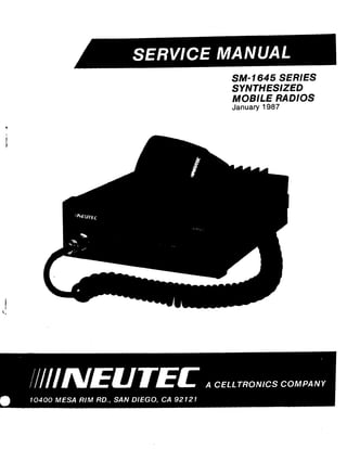
  • 3. SM-1645 Series Mobilesand MobileRepeater This Equipment Meetsor Exceeds the FollowingSpecifications General SM-1645H SM-1645L SM-1645HS Transmitter Weight 144- 174 MHz 16 12 MHz - 30 to +60C 13.8 VDC 9.1 amps .98 amps 50 ohms 5 PPM Dual EPROMS 5 or 12.5 KHz 11.7 x 7.2 x 2.6 inches Frequency Range Channels FrequencySpread Operating Temperature OperatingVoltage Current Drain(TX) Current Drain(RX) Antenna Impedance FrequencyStability Programming Channel Spacing Size 4 Ibs. 2 02s. Specifications subject to change without notice. 136- 174 MHz 16 12 MHz - 30 to +60C 13.8 W C 8.5 amps .8amps 50 ohms 5 PPM EPROM 5 or 12.5 KHz 7.2 x 2.6 x 10 inches RF Output Power Modulation Spuriousand Harmonics Hum and Noise Audio Distortion 30 - 50 MHz 16 2.5 MHz - 30 to +60C 13.8 VDC 9.0 amps .8amps 50 ohms 5 PPM EPROM 5 or 12.5 KHz 7.2 x 2.6 x 10 inches 4 Ibs.2 02s. 45 Watts (adj. 10-50) 16- - 80 dB - 50 dB 3% 45 Watts (adj. 10- 50) 16- - 80 dB -50 dB 3% .25 u V ( 12 dB SINADJ -85 dB - 85 dB - 75 dB - 50 dB 5 Watts 5 Ibs 4 02s. 35 (adj.) 16B - 80 dB - 50 dB 3% .25 uV ( 12 dB SINAD) - 85 dB - 85 dB - 75 dB - 50 dB 5 Watts Sensitivity Selectivity Imageand Spurious IntermodulationRejection Hum and Noise Audio Output .25 UV(12 dB SINAD) - 85 dB -85 dB - 75 dB - 50 dB 5 Watts
  • 4. LOCATIONOFCONTROLS "Transmit" Indicator "Busy" lndlcator 1 pOwerswitchonloff~ Squelch Control and Scanned Channels Designator Microphone Receptacle (with Scan Option) Channel Select OPERATING PROCEDURE 1. Turn the "Volume Control" clockwise to apply 5. When the channel is clear (background noise power. The channel indicator will illuminate. only), rotate the "Squelch Control" clockwise 2. Set the "Channel Select" switch to the desired until the receiver is silenced. Perform this step channel, as shown in the "Channel Indicator" carefully. Donotgo far beyondthesilencingpoint window. or the receiver may not respond to weak signals. 3. Rotate the "Squelch Control'' counterclockwise. 6. After setting the receiver controls and seleaing , 4. Adjust the "Volume Control" for a normal theproperchannel, depressthe microphonepush listening level (background noise or a station if tatalk switch and speak across the face of the one is transmitting). microphone in a normal voice when transmitting. , PRIORITY SCAN INSTRUCTIONS 1. Turn the radio on. 6. Activate the scan mode bydepressingthe "Scan" 2. Selectthrough thechannelsandusethe "Delete/ switch. A t this time the channel display will Add" switch (detent of squelch pot) to delete indicate scanning of the channels in the scan list those channelsthat are to be skipped during the scan sequence. As channels are deleted the tone 7. Verify the priority monitor by opening "Squelch" light will extinguish. on a non-priority channel andnoticing the "look- 3. Set the "Squelch Control" to quiet the receiver. back" action to priority channel. (Thisshould be set on a non-active channel.) 4. Set the "Channel Selector" to the channel that is 8. Reset the "Squelch" to threshold. to be the priority channel. 5. Engage the priority monitor by depressing the 9. Removethe microphonefrom itS brackettoassure "Prioriv' switch. (This step should only be priority channel switching. included if the prioritychannel is to be monitored at all times.) 10. Replace the microphone. -2 -
  • 5. General Transmit and receive frequencies are determined from binary informationstored in the EPROM, IC703. If the MT-20 Multi Tone option is installed, CTCSS Encode and Decode frequencies are also derived from binary information stored in the same EPROM. Datafcr eachchannelconsistsof 16 bytesor memory locations. The first 8 bytes control receive frequency and tone and the second block of 8 bytes control transmit frequency and tone. Each byte or memory locationstores8 bits of data. The upper four bits are tone informationandthe lowerfour bitsarefrequem cy information. If no CTCSS Encode or Decode is programmed, then the upper four bits of each memory location will remain all ones, or, as repre- sented in Hex."F." The transmitor receivefrequency data is strobed into the synthesizer in eight-four bit blocks, via four data linesfrom the EPROM.Thisdata sets the counters internal to the synthesizer so that the appropriate VCO oscillates at the desired fre- quency. The addresses of the data to be sent to the synthesizer are obtained from the Channel Select switch and the TX/RX mode input to the EPROM. Computation of ROM Data: Counter data can be determined mathematically using the formulas shown below. The result of the computations will consist of 8 figures in Hex format for each transmit or receive frequency. The following example for channel 1 is based on a simplex frequency of 154.430 MHz without CTCSS. Note that the receiveHexcode is computed for 21.6 MHz below the desired receive frequency. For l o w band radios 2 1.6 MHz will be added to the receive frequency instead of subtracted. The eight data values for each transmit or receive frequencywill be labeled DO thru D7 and shown in Hex. RECEIVER DATA: VCO freq: 154.430- 2 1.6 = 132.83 MHz N= ( 132.830 x 1000j/ 5 =26566 (5 being the channel spacing) 26566 / 10240 = 2.5943359375 (*) W = lnteger value of above D4 = 2. Multiply figures to the right of the decimal by 16. .5943359375 x 16 = 9.509375 (*) D3 = lnteger value of above D3 = 9 Again multiply fractionary remainder by 16. ,509375 x 16 = 8.15 D2 = 8 Multiply fractionary remainder by2.5 .I50 x 2.5 = 0.375 Dl = 0 Multiply fractionary remainder by 16. .375 x 16 = 6.0 DO=nearestwhole number(ifafraction) which in this case is 6 DO=6 So far we havevalues for DO thru W. The values for D5 thru D7 are determined by the channel spacing. Spacing can be 5 kHz (most U.S. frequencies) or 6.25 kHz spacing (mostly European). This is determinedby whether the frequency is divisible by 5 or 6.25. For 5 kHz steps: M = O D 6 = C D7=3 For 6.25 kHz steps: DS=O D6=O D7=3 The completedata loadfor 154.430MHz(RXJthen is: DO=6, D l =0, D2=8, D3=9, W = 2 , D5=0, D6=C,C7=3or(6 0 8 9 2 0 C 3 ) TRANSMllTER DATA: VCO freq: 154.430 N=f154.430x10001/5=30866 . (5 beingthe channelspacing) 30866 / 10240 =3.0162109375 (*) W = 3 .0162109375 x 16 = .259375 (*) D3 = 0 .259375 x 16 =4.15 D2 =4 .15 x 2.5 = .375 D l = 0 .375x 16 =6.0 DO=6 As before, channelspacing being 5 kHz, then: D5 = 0, D6 = C, D7 = 3 The completedata loadfor 154.430 MHzTX then is: DO=6, D l =O, D2=4, D3=O, W=3, D5=0, D6=C,D7=3or(6 0 4 0 3 0 C 3) It must be rememberedthat in the hexadecimalsys- tem, numbersbetween 10 and 15 arerepresentedby the lettersA thru F. Ifwe were to program 154.430 TX/RX into channel 1, thecompletedataloadfor the first 16addressesof the EPROM would then be: F 6 m F 8 W R , m F C R , f i F O F 4 K ) n , H > F C n Note that the upper 4 bits of each byte at each address will be filled with one's (F), as they are unusedbythesynthesizer.Also, the RXdataisalways entered first EXAMPLE DATA CHART EPROM ADDRESS DATA LOAD FUNCTION REMARKS 00 Do F6 qRX)=I54.430 MHz 01 Dl FO qVCO)=154.430-21.6 02 DZ F8 =132.830 MH7 03 D3 F9 04 W R CHI 05 D5 FO RX 06 D6 FC 07 D7 I3 DO F6 F(TX)= 154.430MHz Dl FO F(VCO]= 154.430 D2 F4 D3 FO w n CHI D5 FO TX FC 137 n ('1 The dwision of N by 10240 and subsequent multiplicationof the fractional panby 16 should be done by hand or computer with appropriate accuracy as these numbers can sometimes extend 12 decimalplacesand must be carried rather than roundedoff so as to maintainaccuracy. -3-
  • 6. CIRCUIT DESCRIPTION RECEIVER General 1st Local Oscillator The SM-1645's double superheterodyne design em- See "PLL/Frequency Generation". phasizes high sensitivity, low noise leveland excellent selectivity.The first IF frequenq is 21.5 MHz and the 2nd second IF frequency is 455 kHz. 0105 isa crystal-controlled oscillatorat 21.145 MHz, RFAmplifler A low-noise, dual-gate FET(0101)amplifies low-level signalsfrom the antenna terminal and feeds the next stage (1st Mixer).RF coils L101-L105 affect the band- width, filter incomingsignalsand preventundesirable radiationof the 1st localoscillator frequency. 1st Mixer This function, performedby 0102, serves to mix the incoming signal and that of the 1st local oscillator, resulting in the 1st IF of 21.6 MHz. This stage is im- portant inachieving a high level of intermodulation rejection. with the frequency fine adjustedby CVIOI.This signal , is fed into the 2nd mixer (0106). Squelch Control Circuit In a noise squelch circuit, the internal noise of the receiver decreases when a signal is present. When there is no incoming signal, noise is picked up and amplified by half of IC102 and part of IC103. It is then rectifiedby 0107 and converted to a DC level. The DC signal is fed to a Schmitt Trigger Circuir (comprisedof the other parts of IC103),which stops the amplification function of lClO2 (DC-Controlled Attenuator). When there is incomingsignal, and the internal noise decreases, the Noise Detector(0107)losesits output 1st IFAmplifler and pin 10 of IC103 goes high, enabling IC102.The This circuit, consistingof 0104, amplifies the 21.6 MHz squelch point is controlled by the squelch potenri- signal. ometer, which varies the gain of lClO2 at the DC level. 2nd Mlxer Busy Llght This function, performed by 0106, serves to mix the Where tone squelch systems are incorporated into frequency of the 2nd local oscillator, and to convert the radio, it is necessary to check for other signals 21.6 MHz to the 2nd IFof 455 Khz. before transmitting. The busy light indicator serves that purpose. 2nd IFAmplifier The busy light functions off the high or low DC level This staqe, containedwithin IC101, amplifiesthe455 at pin 10of IC103via LEDdriver transistor 0108. d KHz 2nd IF. Italso performsthe limiting function. Regulated Power Supply Audlo Detector To keep fluctuations in power source voltage from This circ~it,consistingof IC101 and F103, recoversthe influencing the receiver characteristics, IC105 feeds audio signal from the 2nd IF. regulated voltage to the primary circuits, including oscillator, squelch, RFamplifier and IFamplifier. AF Amplifler IC104 amplifies the audio signal from the previous Switching Clrcult stage to the power level needed to drive the loud Inthe TX mode, the receiversupplyvoltageis removed speaker. by 0109-0110 and 0105-0106.
  • 7. CIRCUIT DESCRlPTlON TRANSMIITER General The oscillator uses a programmable Phase Locked Loop(PLL).The resultantVCO frequency is the same as the channel frequency on transmit and 21.6 MHz below channelfrequency on receive.Inthe transmit mode, the VCO output is modulated, amplifiedand fed to the antenna. PLL, Exciter Boards The circuits that make up the transmitter are: PLL Transmitter Exciter Modulator Power Supply PLL/Frequency Generation Transmitter drive at the carrier frequency and the receiver 1st local oscillator signal (21.6 MHz below the desired receive frequency)are generatedrespec- tively by independent VCOs 0203 and 0201. The signalfrom transmit VCO 0203 is bufferedby0204 before being fed to the TX exciter and PLL buffer 0205. The output from receiveVCO 0201isbuffered by 0202 before being fed to the receiver 1st mixer. In the receive mode, 0201 output is also fed to the PLL buffer 0205 via 0204. The frequencyof the respectiveVCOs are controlled bya DCvoltage derived by the PLLcircuitry.The DC voltage results from a phase/frequency comparison between the divided-down frequency from the ref- erence oscillator controlled by4.8 MHz crystalX2Ol and the divided-down output from the VCO. These functions are performed by the dual-modulus syn- thesizer lC202. XTAL heaters R267 and R268 stabilize the tempera- ture of the reference oscillator. The heating is con- trolled by0214 and 0215, and is proportional to the ambient temperature as sensed by the thermistor TH201. The resultantVCO controlvoltage(andhence frequency) is determined by the divide ratio of the counters internal to IC202. The VCO voltage will vary between 1.5 volts at the lowest frequency and 7.5 volts at the highest.This voltage is generated by 0206,0207 and 0208 based on phase data from the synthesizer IC202. Digital data, which sets the internal counters (or divide-by ratios) i n ICZOZ, is stored in an Erasable Programmable Read-Only Memory(EPROM)IC203. The synthesizer, IC202, requires32 bitsfor frequency determination.Data is transferredor "strobed" into IC202 in eight 4-bit "words" in order to simplify interconnectionand package size. Strobing is done byclockingthe addresses to the EPROMand IC202. The data entering lUO2 via data pins DO-D3 isstored in internal latches as determined by the address present. Address strobing is accomplished by clock IC205, which drivescounter lC204. IC204converts theserial clock pulses from IC205 to 3-line binary addresses between 0 and 7 (decimal)at outputs 00-02. PLLunlock protection is providedby0212 and 0213. This circuit will disable the TX exciter in the absence of lock detect at IC202.A high or "1" is supplied to EPROM IC203 address line 3 (pin 5) during TX in order to switch strobing up by eight addresses. This allowsreceivedata to bestoredinthe first8 addresses and transmit data within the next8 addressesof any given 16 address "channel block" selected by the channel select circuitry. Channel select addressing takes place at address linesA4-A7 of the EPROM. It is conceivable that up to eight 16-channel blocks could be addressed via unused lines A8-A10 for a total of 128 channels. (The 2716 EPROM stores up to 2048 bytes. Each channel requires 16 bytes, which provides room for 128 16-byte "groups".) lC2Ol isadual moduluscounter controlledby IC202. The dual modulus method simplifies overall design byproviding a selecteddivision ratio on the input of IC202. Operating frequency versus VCO voltage is deter- mined by Varicaps D2OI-D2O2 at the receive VCO and D203-D204 at the transmit VCO. Modulation of the transmit VCO is determined by applying the audio signal to Varicap D205.
  • 8. Transmitter Exciter 0209, 0 210 and 0 211 amplify the transmitter VCO signalto asuitableinput levelfor thedriverstage(0.5W). The stages are broadband transformer coupled and do not require tuning. Modulator This stageconsistsof DualOp-Amp IC207.Onehalfacts halfasaspeechamplifierandtheother halfprovidespre- emphasisandlimiting.Appropriatehighfrequencyrolloff is accomplishedbya low-passfilter on the output of the secondstage.Microphonesensitivityisset byVR2O1 and deviation by VR202. Power Circuits TX/RX switching is accomplishedb y 0 217and0 216.In thereceivemode, 0 217saturatesasaresultofbasedrive from 8 V regular IC206. Saturation of 0 217 providesa ground path for RX VCO 0 2 01, thereby enabling it. Shortening the PlT line to ground shunts base drive to 0 217, w5ich prevents it from conducting.This, in turn, disables RX VCO 0 2 0I . In this condition, base current flows through 0 216, causing it to saturate and to pro- vide +8 V DCtothemodulator, TXVCO andRFpredriver 0209 via 0213, which is part of the lock detection circuit. Voltage regulation is providedby IC208 (+5 V DC for the logic) and IC206 (+8 V DC for modulator and TX v c o j . DisplayBoard A 7-segment 2digit LED is used to display the channel beingused.FouradditionalLEDsserveto indicatevarious functions of the radio. The channel select switch sends out positive logic 4-bit binarycodesrepresenting0 to 15 decimal.To convertthis to 1 to 16, "1" is addedto the 4-bit code output by4-bit parallel full adder lC6O1. IC602convertsthe 5-bit binarycodefrom the adder to 2-digit BCD for the display. The upper digits are 0 to 1, with 1 indicatingCh. 10toCh. 16.The 1-bit outputofthe upperdigits isconnectedto 0 6 01, which drives theseg- ment that corresponds to "1 " on the first digit of the 7-segment display. BCD codes for the lower digits are connectedto IC602, which drives the second digit of the 7-segment display. The +-bit codes from the channel select switch are also fed to the EPROM on the synthesizer board. CIRCUIT DESCRIPTION ADDITIONAL RECEIVER PLL/REPEATER CONTROL PCB (SCHEMATICON PAGE 41) SM-l645HS Duplex Mobile Repeater The receiver PLL PCB has two functions. It must 3 linebinaryform, isprovidedbycounter IC704 which separate the first local oscillator siqnal for the receiver is driven by free running clock consisting IC 705. independently of the transmitter ~ C Oso as to allow meRx PLiPCB contains additional circuitry which Operation* and it Conuo's Operation Of the controls ifthe isto operate intheduplex modeor transceiver in the duplex mode or as a repeater. repeater mode, and also provides an audio path The VCO/synthesizer circuitry is identical to the transmitter VCO/synthesizer which was previously described and which is contained within the exciter PCB. Inthe receiver PLL section ,the VCO function is performed by 0 7 01. The output of 0 7 01, which is 21.6 MHz below the desired carrier (channel) fre- quency, is fed to buffers 0703 and Q702. The output of 0703 is fed to the Rx first mixer on the Rx PCB. The output of 0702 is fed to PLLbuffer 0704. The output of 0704 is fed to IC 701. IC 701 is proqrammable between the Tx and Rx when in the repeat mode. Control is accomplished by IC 706 and IC 707. Repeater/duplex selectionisdeterminedbythe levelof J701 pin9. A highatthispoint selectsrepeater while a lowselectsduplex Q 708 providesaudio feedto theTx byamplifyingandde-emphasizingthe Rxdiscriminator signalfrom the RxPCB. Deviationinthe repeatmode is controlledbyVR 701, audio pathfrom themicrophone (duplex mode) or the Rx PCB (repeater mode) is selected by analog switches in IC 708. N/N+ I variable modulus counter whose countins Tx activation inthe repeater mode is controlled by the ratio iscontrolledbysynthesizer IC702. The outputof squelch level from the Rx PCB (COR). Additional IC702 isusedtocontroltheVCOasdeterminedbythe circuits on the PLL PCB are voltage regulation as binary data loaded into receive EPROM IC 703. The provided by IC 708, IC 709. Reference oscillator xtal binary data in IC 703 is clocked into the internal X 701 istemperature stabilized byproportional heater counters of the synthsizer IC. Promaddressingdata, in circuit consisting of Q 710 and O 71 1.
  • 9. MT-10CTCSS SINGLE TONE ENCODE/DECODE OPTION (SCHEMATICONPAGE43) General Theory MT- I0 InterconnectTable: Neutec's MT-10 Single Tone option equips the Pin: Function: Destination: SM-1645 seriesofmobileradiosfor operationinCTCSS ~ 9 0 environments. With this option, the radio canencode I Groundingjunction at or decode anyof the38 EIAstandardtones. Program volume pot ming of tone information is accomplished via dip +5 VDC switches. MT-10 Single Tone option can not be used +5 VCD output from PLL with SC- 10 Scan Option Bd. (P2027) Input/Output Functions: DECODE ENABLE [J901-4) - This input disables the audio gate on carrier channels until a carrier signal is detected. For tone channels, this input is ignoredand audio is allowed to pass only after the proper tone is detected. MONlTOR ENABLE (J901-6) - When the micro- phone is removed from its bracket this input is removed from ground. This opens the audio gate, allowing the selected channel to be monitored for activity. TX TONE OUT (J901-7) - The programmed CTCSS tone is sent to the exciter via this output (Adjustment allows for proper deviation control.) TX ENABLE (J901-8)- This input providestransmit enableto the tone chip. Thiswill causethe tone signal to be sent to the transmitter circuitry. 3 Audio In Receiver Bd. Detector (PI02- 1j Pin closest to front of unit 4 Decode Enable Receiver Bd. Sq. Detect (IC103-10) - 5 Audio Out Receiver Bd. Audio Amp (PI02-2) Pin farthest from front of unit 6 Monitor Enable Mic Hook-Switch 7 TX Tone Out PLIJExciter Bd. (VR202 wiper)* Tone Programming: 8 TX Enable Solder to gray wire on Tone selection is accomplished by setting the dip switches on the Tone Boardas indicatedinTone Data J401 of driver board (PF). Table. Installation: 1. A wiring harness for scan and tone options is incorporated in Neutec mobiles to facilitate field installationor exchange. 2. Locateand secure MT-I 0 Tone Board inthe space provided next to the internal speaker, on top side of radio. 3. Remove green jumper from Receiver Board J102 and connect two pinplug from wiring harness. 4. Connecteightpinplugfromwiring harnesstoJ901 of MT-I0 Tone Board. 5. Onbottomsideofradio, connectfour pinplugfrom wiring harness to four pin plug provided. Solder oppositeendofwire toJ401 pin4 onDriverBoard. Alignment: TX TONE LEVEL(R7)-With the transmitter keyedon a tone channel, adjust R7 for proper sub-audible deviation of the transmitter signal..[Typically+SO0 Hz deviation.j MT- I0SingleToneCTCSSInstallationDiagram: TOP VIEW J901 I Ground, Blk 2 +5 VDC, Red 3 Audio In, Grn 4 Decode Enable. Brn 5 Audio Out Org 6 Monitor, Yel 7 TXTone Out VL 8* TX Enable, Blue Tone Data Table: TONE FREO. TONE # 1Hz) 1 67.0 2 71.9 3 74.4 4 77.0 5 79.7 6 82.5 7 85.4 8 88.5 9 91.5 10 94.8 1 1 97.4 12 100.0 13 103.5 14 107.2 15 110.9 16 1 14.8 17 1 18.8 18 123.0 DATA D2 D3 1 1 1 1 1 1 1 1 1 1 1 1 I 1 1 1 0 1 1 1 0 1 1 1 1 1 1 I 0 1 0 1 0 1 0 1 156.7 0 1 1 0 1 0 162.2 0 1 1 0 0 0 167.9 1 0 1 0 1 0 173.8 1 0 1 0 0 0 179.9 0 0 1 0 1 0 186.2 0 0 1 0 0 0 192.8 1 l 0 0 1 0 203.5 1 1 0 0 0 0 210.7 0 1 0 0 1 0 218.1 0 1 0 0 0 0 225.7 1 0 0 0 1 0 233.6 1 0 0 0 0 0 241.8 0 0 0 0 1 0 250.3 0 0 0 0 0 0 *NOTE: 1 =OFF 0 = O N
  • 10. General Theory Neutec's MT-20 MultiTone option equips the SM-1645 seriesofmobileradiosfor operationinCTCSS environments. With this option, the radiocan encode or decode any of the 38 EIA standard tonel Tone information is stored inthe single EPROM; alongwith frequency data. Any given channel can be p r o grammedto encodethe transmitter, decodeincoming signalsfor proper tone, or operate ina carrier squelch mode. This universalcapabilityenhances the versatile features of the Neutec product line. Input/Output Functions: DECODEENABLE(J901-4) -This inputdisablesthe audio gate on carrier channels until a carrier signal is detected. For tone channels, this input is ignoredand audio is allowed to pass only after the proper tone is detected. MONITOR ENABLE (J901-6) - When the micro- phone is removed from its bracket this input is removed from ground. This opens the audio gate, allowing the selected channel to be monitored for activity. TX TONE OUT (J901-7) - The programmed CTCSS tone is sent to the exciter via this output (Adjustment allows for proper deviation control.) TONE DECODE OUT (J901-8)-This output is only usedon radiosequippedwith the SC-10, PriorityScan Option. When used, this outputcausesthe scannerto halt when the proper tone is detected. TONECHANNEL(J902-1j -Thisoutput isonlyused on radios equipped with the SC-10, Priority Scan Option. When used, this output informs the Scan Boardthat atone channelhasbeenselected.TheScan Board then extends the sample time to allow for sufficient decode time. DATA IN(J902-2)-Incomingmemorydatafromthe EPROM is input to the Tone Board at this point The serialdata isthen latchedand fedto the tone chip ina parallelfashion. Thisdataacquaintsthetoneprocessor with the programmed tone and options that have been selected. WRITE DISABLE(J902-3)- Data is allowed to enter into the Tone Board only during periods when the write disable line is inthe low state. This actionallows the serial data to be clocked into the Tone Board for instruction processing. AO - AZ (1902-4, 5, 6) - These inputs to the Tone Board set-up the proper addressing of incoming data. eight bits of data. The upper four bits are tone information and the lower four bits are frequency information. When loading an EPROM with the Stand Alone programmer, obtain data DO thru DS from the Tone Data Table. Obtain data D6 and D7 from the Tone FunctionTable below. Tone FunctionTable: Rx Tx Mode D6 0 7 W D7 Rx DecodeOnly 0 F 0 F Tx EncodeOnly F F F 0 Carrier Squelch F F F F 0 F 0 0Encode& Decode The following example for channel 1 is based on a simplex frequency of 154.350 MHz with a CTCSS Encodeand Decode tone of 67.0 MHz. From the Tone Data Table DO-DS are as follows: DO=l D l = l D2=1 D3=1 D4=1 D5=1 Fromthe Tone FunctionTable, receivevalues are: D6=O D7=F Also from the Tone FunctionTable, transmit values are: D6=O D7=0 The complete example data appears below. EXAMPLE DATA CHART EPROMADDRESS DATA LOAD FUNCTION REMARKS 00 DO 16 01 Dl 10 02 D2 18 03 03 19 04 W 12 CH I 05 DS 10 Rx 06 D6 OC 07 0 7 R 08 W 16 09 Dl 10 0A D2 14 OB D3 10 OC W 13 CH 1 OD D5 10 . Tx OE D6 OC OF D7 03 (Tone lnformatim Freq. Informadon) Installation: 1. A wiring harness for Scan and Tone Options is incorporated in Neutec mobiles to facilitate field installationor exchange. 2. Locateand secure MT-20 Tone Boardinthe space provided next to the internal speaker on top side of radio. Tone Programming: CTCSS Encode and Decode information is stored in 3. Remove greenjumper from Receiver Board J1O2 EPROM IC203. on the PLL Board. Each channel and connect two pin plug from wiring harness. assignmentconsists of 16bytes or memory locations. 4. Connectwiring harness eight pin plug to J901 of The first eight bytes are for receive and the second MT-20 Tone Board. Connectwiring harnesssix pin blockofeightbytesarefor transmit Eachbytecontains -8- plug to J902 of MT-20 Tone Board.
  • 11. MT-20 CTCfS MULTITONE ENCODE/DECODE OPTION MT-20 InterconnectTable: MT-20 MultitoneOption InstallationDiagram: Pin: Function: Destination: J901 1 Ground Groundingjunction at volume pot 2 4-5 VDC f 5 VDC output from PLL Bd. (P202-7) 3 Audio In Receiver Ed. Detector . (PI02-1) Pin closest to front of unit 4 Decode Enable Receiver Bd. Sq. Detect (IC103-10) Tone Channel Data In Write Disable A0 A1 AZ TOP VIEW IJ90 1 1 Ground 2 +5VDC 3 Audio Iln 4 Decode Enable 5 Audio Out 6 Monitor 7 TX Tone Out 8 DecodeOut 5 Audio Out Receiver Bd. Audio Amp Alignment: (PI02-2) Pin farthest from TX TONE LEVEL(R7)-With the transmitter keyedon front of unit a tone channel, adjust R7 for proper sub-audible 6 Monitor Enable Mic Hook-Switch. deviation of the transmitter signal. (Typically +500 Hz deviation.) 7 TX Tone Out PLwExciter Bd. (VR202 wiper)* 8 Tone Decode Scan Bd. (J803-2) Out Only used with Scan Board option. J902 1 Tone Channel Scan Bd. (J803-3) Only used with Scan Board option. 2 Data In PLL Bd. (J205-1) 3 Write Disable PLL Bd. CKl (J203-2) 4 A0 PLL Bd. EPROM(1QO3-8) 5 A1 PLL Bd. EPROM (IQ03-7) 6 A2 PLL Bd. EPROM(lC203-6)
  • 12. SC-10 PRIORITYSCANNER OITION (SCHEMATICON PAGE47) GeneralTheory The SC-1 0 Priority Scanner Option for the SM-1645 Series of mobile radios allows scanning of all, or any portion of, programmedchannels. Designed to offer simple, effective operation, the SC-I option will aute maticallystop scanningwhenever activity isdetectedon an enabled channel. Channelsare enabledintwo methods. First the initial scan list length is established by ajumper on the scan board. This jumper may be installed to establish a scanning list for 2 to 16 channels. Secondly, once the scan list is set the user can delete/add channelsvia a switch on the front panel. Addition or detection of a channelisaccomplishedbyturningthesquelchcontrolin to andout of the CH IN/OUT position.the CH/IN light indicates whether the channel is in the scan list. Priority channel monitoring is accomplised by activb tion of the priority on/off push button. this feature assures that the priority channel is always monitored - even during activity on non-priority channels. A "priority-check" monitor constantly samples the prioritychannelto detectactivity. Ifactivityisdetected, the scanner will immediately revert to the priority channel and maintain that channel until activity is concluded. Input/Output Functions: DO - D3 INPUTS- Channel selection is input to the scanboardat U2.Whenthescanoption isdisabledthe input data is passed to the output via the data bus. When the scan modeisengagedthe data isclockedto artificially advance the channel selection. Whenever the priority channel monitor detects activity on the priority channel, U2 again passes the direct data information as output to the display and synthesizer boards. 61T 0 -' BiT 3 OUTPUTS - These outputs control the display logic and synthesizer.'When the scan mode is off, these outputs fallow the DO - D3 inputs. Upon scan activation, these outputs are artificiallyadvanced by the scan clock circuitry. CH/IN LIGHT OUTPUT - To indicate scan list selec- tion the tone light is illuminatedon channelsthat have beenselectedactive.As channelsare deleted the tone light is extinguished. SCANON/OFF INPUT- The"Scan" switchappliesa ground to the scanenable input Thisenablesthe scan mode and allows U2 to pass the clocked artificial channel data. PRIORI7Y ON/OFF INPUT - When the "Priorit)/' switch isclosedthepriority monitor isenabled. During priority monitor condition U2 periodically reverts to manualmodeto allow the synthesizer to momentarily lock-on to the priority channel. If activity is detected the scan sequence is halted until activityconcludes. If the priority channel is inactive, the scan sequence resumes at the previous channel. CARRIER INPUT-The not carrier input enables the , scanclockoscillator. Whenacarrierisdetectedthisline isforcedlowcausingthescanclockto bedisabled. The scan sequence will then continue when the carrier is . removed. TONE CHANNEL INPUT-The not tone line is input from the tone board (TS-2). This line is forced low whenever a tone channel is scanned. When a tone channel is scanned (anda carrier is present) the scan cycle time is increasedto allow sufficient time for the tone board to detect tone information. If the proper tone isdetectedbythe tone board, the scansequence ishalted until the tone is removed. (Whenthis input is unused the line should be connected to 4-5volts.) DECODEINPUT-When the tone board detects the proper CTCSStone, the not decode line is forced low. This disables the scan sequence until the tone is removed. DELETE/ADD SWITCH - This input is momentarily grounded to toggle the selected channel in or out of the scan list Scan List Length Programming: The SC-1 can be programmed to scan from 2 to 16 channels. Programming is accomplished by installing . jumper J1. Installthejumper to theprogrampointand the position which directly corresponds to the maxi- mum desired channel number. PROGRAM 12 IS 14 9 8 1 1 10 . . . . . .
  • 13. Installation: 1. A wiring harness for Scan and Tone Options is incorporated in Neutec mobiles to facilitate field installation or exchange. 2. Locate and secure SC-10 Scan Board in the space provided on bottom side of radio. 3. Removejumper from wiring harness eight pin plug and connect eight pin plug to Scan Board J903. Connect wiring harness six pin plug to Scan Board J902. Connectwiring harnessfour pin plug to Scan BoardJ901. 4. If MT-20 Multi Tone Board is not installed B03 pin3, tone channel, mustbeconnectedto 4-5VDC. Scan Board InterconnectTable: Pin: Function: Destination: J903 1 DO Channel Selector 2 Dl Channel Selector 3 D2 Channel Selector 4 D3 Channel Selector 5 Bit 3 Orange/White wire from channel selector 6 Bit 2 Red/White wire from channel selector 7 Bit 1 Brown/ White wire from channel selector 8 Bit 0 Black/White wire from channel selector J902 1 InList LED Amber Tone Light cathode 2 Priority Sw. Priority Switch (center contact) 3 Scan On/Off Scan Switch (top contact) 4 Delete Sw. Switch contact at back of Squelch Sw. 5 4-5 VDC +5 VDC output from PLL Board (J202-7) 6 Ground Ground lead from PLL Board (J202-2) J901 i Carrier Receiver Board IC103 pin 8 2 Decode MultiTone Board (J901 pin8)* 3 Tone Chan. MultiTone Board (J902 pin 1)** 4 Priority Sw. Priority Switch (top contact) SC- 10 PriorityScanner Board Installation Diagram: Channel PLL & Display Selector 1 Board CH IN/OUT SW +s VDC Ground J902 SCAN BOARD [I;Priority Enable SW Tone Channel Decode Carrier 1 Notes: *I. For units without MultiTone, J901 is unused. **2. For units without MultiTone, J901 should be connected to +5 VDC.
  • 14. Parts Variationvs FrequencyChart 30- 50 MHz PLL& Exciter Receiver C-101 C-105 C-110 C-1 13 C-1 16 C-120 C-123 Driver & APC -I I 4.7 ohms %W 20 ohms 2W - 1 0 K S W 100 ohms 2W 8 2 K S W 30 - 35 MHz 33P CH 33P CH 33P CH 33P CH 33P CH 25P CH 25P CH I I Power Amplifier 40 - 45 MHz 33P CH 25P CH 25P CH 2SP CH 25P CH 15PCH 15PCH 35 - 40 MHz 33P CH 33P CH 33P CH 33P CH 33P CH 2OP CH 2OP CH - 1SOP CH 300P SL 300P SL 300P SL 1OOP CH 1PCH 36P CH 3P CH 39P CH 5P CH 5P CH 39P CH 3P CH 36P CH l P C H 45 - 50 MHz 20P CH 2OP CH 2OP CH 2OP CH 2OP CH 12P CH 12PCH
  • 15. Parts Variation vs FrequencyChart 138- 174 MHz The following componentsshouldbechangedto the indicatedvalueswhen the frequencyspreadisother than 148- 165 MHz. Driver & APC C401 C403 C407 C411 others 160- 174 MHz not used not used 2OpF cer. not used not used *Note 1. 148 - 165 MHz 1pF cer. Receiver Cl02 C104 C109 C l l 2 Cl 15 Cl2l C124 not used not used not used not used *Note 1. 138 - 148 MHz 4pF cer. not used Power Amplifier Note. 1 Shunt a 220 ohm % watt resistor between C402 input side and ground. Nore 2. Shunt a 30pF ceramic capacitator between the collector of 0 5 01 and ground. C506 C507 others not used 39pF cer. *Note 2. not used not used
  • 16. VCO Connect a wattmeter and a dummy load of suitable dissipatior;to the antenna connector. Connecta high impedance voltmeter to test point CPZOI, which is locatednext to the shielded area (VCOs)on the syn- thesizer/exciter board. (NOTE:With the PLL/exciter board uprightandwhile facing the front of the radio, you will see the RX VCO coil on your left and the TX VCO coil on your right within the VCO shielded area. CP2Ol is to the right of the coils.) Adjust the RX VCO (L201)for about 4 V DC while on a channel which is approximately in the center of the desired frequency range. Readjust I201 to obtain no less than 1.0 V DC on the lowest operat- ing frequency and no more than 7.5 V DC on the highest. (NOTE:Itis importantthat the VCO coilsbeadjusted carefully and with the proper tuning tool to avoid damaging the core. Itisalso importantthat the friction locking rubber piece insertedbetween the core and the coil be in place to eliminatethe possibilityof the VCO falling outside the 1.0 to 7.2 volt rangeduring vibration or movement.) After adjusting the RX VCO, activate the transmitter and adjust the TX VCO coil (1202) in the same manner. ~djust'thereferenceoscillator trimmerVC2Ol for the correct carrier frequency at the selectedchannel. Transmitter Begin transmitter alignment by setting VR401 to its full clockwise position. Then transmit on a frequency that is near the center of the radio's assigned fre- quency range, and adjust the driver's input and output tuning capacitors, (VC401, VC402) for maximum output. Now adjust the input and the output tuning capaci- tors for the final stage (VC501 and VCSOZ) for max- imumoutput These can be reachedthrough holeson the final P.A shield. Alternate tuning VC401, VC402, . VC501 andVC502 for maximumoutput power. After adjusting transmitter to maximum power, adjust VR401 counter-clockwise until power drops slightly. (Note: To ensure proper power output use a power supplycapableof supplying13.8 VDC at 10ampsand heavy power cables.) While modulating the transmitter, set deviation to 4.8 KhzbyadjustingVR202 (locatedon the PUboard at the end opposite the synthesizer and the PROM ICsJ.Next, adjust mikegain potentiometerVR2Ol for proper deviation while holding the microphone at the desired speaking distance. Receiver Select a channel on the approximate center of the desiredoperating range. To the antenna connector, connect a signal generator modulated by a 1 Khz tone set for 3.3Khzdeviation. ConnectaSINADmeter to the external speakerjack on the rear of the radio. Turn squelch control fully cownterclockwise.Adjust: LlOl through L107 for best SINAD while maintaining the output of the generatorclose to the 12 dB point. Readjust coils as necessary for proper receiver responseover the operating range. IFcoils L108 through Lll2 come properlytuned from1 the factory. It is not advisable to tamper with the tuning. If it becomesnecessary, however, follow the SINAD methoddescribedabovefor front-endtuning. The 2nd local oscillator, although not usually necessary, canbe set byconnectinga high sensitivity frequency counter to test point CPlOl on the RX PCB andadjusting CVlOl for 21.145 MHz.
  • 17. Top View - 15-
  • 19. TROUBLESHOOTINGAND 'SUGGESTEDTEST EQUIPMENT It is recommendedthat maintenanceof the radiobe done at the board exchange level. Service facilities can take maximumadvantageof the boardexchange programbystocking a set of replacementboardsand by returning defective boards to the factory. The transceiveriscomposedof fiw boardsthat contain all of the circuitry.Any malfunctionshouldbe isolated to a board and verified by an exchange. The five boards are: PLLSynthesizer/TX Exciter Receiver RFdriver RF power output Display . Exceptfor the Displayand RFP.A., these boardscan be removed and replaced with a screwdriver and some care. the RX VCO is operating, then most RX malfunctions would be a result of a problemon the receive board. Transmittermalfunctionscouldbeonanyoneof three boards.As with the receiver, the first place to check would be the TX VCO voltageat CP2Ol while inthe TX mode. Ifthis voltage iscorrect, the problemcould be inthe predriver, driver or power amplifier stages. To isolatea transmitterproblem, firstcheck the power supplycurrent during transmit. As the driver draws approximately2 amps, failureof the finalstage would show some increase in current during transmit (about 2 amps more than while receiving). Little change in current between TX and RX would indi- cate problems in the predriven(PLL board)or driver (assumingthe TX VCOwas operational, whichshould be the first test). An additional test could be made with an RF probe or an RFvoltmeter at the input to General the driver stage (about 5 volts RMS should be present here).Output of driver stage should be 8.0 The PLL Synthesizer/TX exciter board contains the or more wical,. modulator, RX and TX VCO, TX predrivers and synthesizer circuits. As such, a receive malfunction Modularconstructionof the transceiver was intended couldbean RXVCO problemonthe PUboard.Proper to simplify servicing at your facility as this can be a VCO operation can easily be verified by checking hiddencostassociatedwithother transceiverswhere for 1.0 to 7.2 volts at the VCO test point CP201. If troubleshooting mustbe pursuedto the component level. Test Instrument RequiredSpecifications SuggestedType DC Power Supply Voltage: 13.8 VDC Current: 10Amps Cont. Astron RS-12 RF Watt Meter Frequency 136-174 MHz Bird Model43 Powec 0-100 Watts With 10 C Element Impedance: 50 Ohms - - - RF Dummy Load Impedance: 50 Ohms Bird Model 8085 or Power 50 W Model 8341-200 DC Voltmeter Range: 0-15 V Simpson260 and DC Input Resistance 10 Meg Ohm Data Precision1351 AC Voltmeter Range: 3 mV-I0 V Leader LMV 181A Deviation Meter Range: 0-5 KHz Marconi TF 2304 +/- DeviationCapability FrequencyCounter Range: 136-174 MHz Accuracy: +2 ppm/yr HP5383 A or Data Precision5000-TB8 RF Signal Generator Range: 136-174 MHz Wawtek 3005 Level: 0.1-1000 uv Modulation: InternaVExternal Deviation: 0-5 kHz -- Speaker Load Impedance:8 Ohm Power: 7.5 Watts Min. With SwitchSelectable Int.8 Ohm Speaker Shop Fabricated
  • 20. -8V 0206 -5V rn 6n x 0 5GI VCO -- CONTROL ' i +BV +BV +BV -5v -5v +5v 0205 IC201 t lC202 IC203 r - ------------ N - : CHSELECT -4 RX VCO TO RX PLL N + l -SYNTHESIZER - EPROM (DISPLAY I BUFFER bDt$l-f-lt~ SWITCHLOCK * 0214-0215 M IC -.*.. DEV 1GAIN .' SET 1'2207 TX COUNTER 1 O A R ! , - MIXER I 1 l A TXB+ +8V i-, TX TX VCO BUFFERVCO I A 0, I XTAL HTR - L - - - c,----------J '7;AG~s,1'2205 ADDRESS GENERATOR CLOCK 13 8V 138V 0209 0 2 1 0 0211 b 1 3 8 V B+ IC208 - IOSW) A 0213 RF TX RF AMP OUT SPEECH LIMITER ' NEUTEC COMMUNICATIONS INC. 0216 +5V 4 -- RF- AMP -- - OUT OF 5v REGULATOR -0217 RF AMP REGULATOR + SM-1645 MOBILE TX B+' (8V) TXB+ SWITCH L RX VCO ENABLE PLLIEXCITER BOARD RX VCO SWITCH IC206 +8V 4 8V
  • 21. 0101 0102 0104 0106 r 1 ANT INPUT RF 1st 1st IF 1st IF , 2nd . 2nd IF (From Final PCB) - AMP MIXER FILTER AMP MIXER FILTER I RX VCO NEUTEC COMMUNICATIONS INC. SM-1645 MOBILE RECEIVER BOARD I IC101 IC102 IC104 2nd IF/ DETECTOR I IC102 1C103 0107 IC103 Dl04 0 108 SO CONTROL I AF OUT VOL CONTROL I ' - NOISE DET NOISE AMP , , SCHMITT TRIGGER AF SWITCH SW BUSY LT
  • 22. BLOCK DIAGRAM NEUTEC COMMUNICATIONSINC. SM-1645 MOBILE DISPLAY BOARD MSD 0601 25'22724 SL2271 LSD INDICATOR IL TO PLL + LED DRIVER 4 I IC601 IC602 IC603 CH SW I 74LS283 74185 74LS47 D604 ElBINARY CODE I - - -I 7 BCD TO 7SEGMENT 3 ' BINARY TO BCD I 4 I I-, 1 . 16 4 0 - 1 5
  • 23. NEUTEC COMMUNICATIONS INC. SM-1645 MOBILE DRIVER BOARD DRIVER (0.5W) PTT TX RF 8+ DET TO P.A. PCB TO PWR CONTROL CKT ~ ~ - ~~- ~ FINAL PWR AMP BOARD RF IN (low) 7 RF PWR AMP _ A A - PIN DIODE SW D5W B t TX ' B+ L.P.F. I D510 - PWR DETECTOR ANT
  • 29.
  • 31. SCHEMATIC RECEIVERBOARD 136- 174 MHz 8201-4-IA -29-
  • 33. FT501 0.01 w h C506 !g 1OOOP SLl00P He'C507 2 - .l 9 0 d T10,,/16 $ = a C508 3000-25 0.001 *+ C509 FT502 C535 r 0.01 w m 1OOOP 0 P P 0 J C510 - SL300P +-l+ X E C511 R506 p x z g C H l O O P ~ ~ ' 1K -100P 3 ' , VC502 0.01 R502 CH501 1000 2 W 3.9rr CH502 3.9!t C532 470Q 3.911 R509 2 0 0 1W ~530-
  • 35. SCHEMATIC FINAL POWERA M P BOARD 136- 174 MHz PCB8201-4-SA -33-
  • 37. SCHEMATIC DRIVER BOARD 30- 50 MHz LOW BAND DRIVER & APC AMP t 13 6 V For TX ANTSW P T T PWR M T G
  • 39. SCHEMATIC DRIVER BOARD 136 - 174 MHz TX Driver & APC Board Schem. PCB 8201-4-4A PTT POWER DET GND
  • 45. +5 8730 o n 0930 OTONE DECODE -- 0 ,i.Tlr;h # ~ T ~ F + ~ ~ o ~ I ~ Y D C , P O = 680, ~1o2dfi9733
  • 47.
  • 50. PLL/TX EXCITER PCB PARTS LIST REF IC201 202 203 204 205 206 207 208 TYPE DESCRIPTION IC SP8793 IC MC145146 IC 2716 with Socket IC MC14161BP IC MC14069UBP IC TA78L008 IC MC1458 IC 7805 PART # 07-8793 07-5146 07-2716 07-4161 07-4069 07-8008 07-1458 07-7805 REF TYPE DESCRIPTION PART # Heat Sink RF connector RF connector Minipin jack A1 Minipin jack A1 PCB connector PCB connector PCB connector PCB connector PCB connectorFET Transistor FET Transistor FET Transistor Transistor Transistor Transistor Transistor Transistor Transistor Transistor Transistor Transistor Transistor Transistor Thermistor % w Resistor % w Resistor % w Resistor % w Resistor % w Resistor % w Resistor % w Resistor % w Resistor % w Resistor % w Resistor % w Resistor % w Resistor % w Resistor % w Resistor % w Resistor % w Resistor l/q w Resistor % w Resistor % w Resistor % w Resistor % w Resistor % w Resistor % w Resistor % w Resistor % w Resistor % w Resistor % w Resistor % w Resistor % w Resistor % w Resistor % w Resistor % w Resistor % w Resistor % w Resistor % w Resistor % w Resistor % w Resistor % w Resistor % w Resistor % w Resistor l/4 w Resistor % w Resistor % w Resistor % w Resistor % w Resistor % w Resistor % w Resistor % w Resistor % w Resistor % w Resistor % w Resistor % w Resistor % w Resistor Vari-Cap Vari-Cap Vari-Cap Vari-Cap Vari-Cap Vari-Cap Zener Diode Zener Zener Zener Diode Diode Transformer AK-10 Transformer AK-10 Transformer AK-11 lnductor lnductor lnductor lnductor lnductor lnductor lnductor lnductor lnductor lnductor lnductor Variable capacitor 20Pf Variable Resistor IK POT Variable Resistor IK POT X'tal 4.8MHz HC18/u
  • 51. -- -- - - - PART# IREF TYPE -- - PART #REF TYPE DESCRIPTION I/, w Resistor w Resistor 1!,w Resistor I/, w Resistor 1!,w Resistor I/, w Resistor I/, w Resistor 11, w Resistor I/, w Resistor 1/,w Resistor I/, w Resistor w Resistor I/, w Resistor 1 w Metal Film 1 w Metal Film w Resistor w Resistor 1/I w Resistor 1/4 w Resistor % w Resistor C233 Tantalum capacitor 234 Tantalum capacitor 235 Ceramic capacitor 236 Ceramic capacitor 237 Ceramic capacitor 238 Ceramic capacitor 239 Ceramic capacitor 240 Ceramic capacitor 241 Ceramic capacitor , 242 Ceramic capacitor 243 Ceramic capacitor i 244 Ceramic capacitor 245 Ceramic capacitor 246 Ceramic capacitor 247 Electrolytic capacitor 248 Ceramic capacitor 249 Ceramic capacitor 250 Electrolytic capacitor 251 Ceramic capacitor 252 Ceramic capacitor 253 Ceramic capacitor 254 Electrolytic capacitor 255 Ceramic capacitor 256 Electrolytic capacitor 257 Mylar 258 Ceramic capacitor 259 Electrolytic capacitor 260 Electrolytic capacitor 261 Mylar 262 Mylar 263 Mylar 264 Mylar 265 Electrolytic capacitor 266 Ceramic capacitor 267 Ceramic capacitor 268 Ceramic capacitor 269 Electrolytic capacitor 270 Electrolytic capacitor C201 Ceramic capacitor 202 Ceramic capacitor 203 Ceramic capacitor 204 Ceramic capacitor 205 Ceramic capacitor 206 Ceramic capacitor 207 Ceramic capacitor 208 Ceramic capacitor 209 Ceramic capacitor 210 Ceramic capacitor 211 Electrolytic capacitor 212 Ceramic capacitor 213 Ceramic capacitor 214 Ceramic capacitor 215 Ceramic capacitor 216 Ceramic capacitor 217 Ceramic capacitor 218 Ceramic capacitor 219 Ceramic capacitor 220 Ceramic capacitor 221 Ceramic capacitor 222 Ceramic capacitor 223 Ceramic capacitor 224 Ceramic capacitor 225 Ceramic capacitor 226 Ceramic capacitor 227 Ceramic capacitor 228 Ceramic capacitor 229 Ceramic capacitor 230 Ceramic capacitor 231 Ceramic capacitor 232 Tantalum capacitor .022pF SL 1OOP 33uF 16V C225A Ceramic capacitor C264A Electrolytic capacitor C231A Ceramic capacitor
  • 52. RECEIVER PCB PARTS LIST REF TYPE - DESCRIPTION PART X QlOl 102 103 104 105 106 107 108 109 110 RlOl 102 103 105 106 107 108 109 110 111 112 113 114 115 116 117 118 119 120 121 122 123 124 125 126 127 128 129 130 131 132 133 134 135 136 137 138 139 140 141 143 144 Transistor Transistor Transistor Transistor Transistor Transistor Transistor Transistor Transistor Transistor Diode Diode Diode Diode Diode Diode Resistor Resistor Resistor Resistor Resistor Resistor Resistor Resistor Resistor Resistor Resistor Resistor Resistor Resistor Resistor Resistor Resistor Resistor Resistor Resistor Resistor Resistor Resistor Resistor Resistor Resistor Resistor Resistor Resistor Resistor Resistor Resistor Resistor Resistor Resistor Resistor Resistor Resistor Resistor Resistor Resistor - - - -- REF TYPE -- DESCRIPTION PART # Resistor Resistor Resistor Resistor Resistor Resistor Resistor Resistor Resistor Resistor Resistor Resistor C101 Ceramic capacitor 102 Ceramic capacitor 103 Ceramic capacitor 104 Ceramic capacitor 105 Ceramic capacitor 106 Ceramic capacitor 107 Ceramic capacitor 108 Ceramic capacitor 109 Ceramic capacitor 110 Ceramic capacitor 111 Ceramic capacitor 112 Ceramic capacitor 113 Ceramic capacitor 114 Ceramic capacitor 115 Ceramic capacitor 116 Ceramic capacitor 117 Ceramic capacitor 118 Ceramic capacitor 119 Ceramic capacitor 120 Ceramic capacitor 121 Ceramic capacitor 122 Ceramic capacitor 123 Ceramic capacitor 124 Ceramic capacitor 125 Ceramic capacitor 126 Ceramic capacitor 127 Ceramic capacitor 128 Ceramic capacitor 129 Electrolytic capacitor 130 Ceramic capacitor 131 Ceramic capacitor 132 Ceramic capacitor 133 Ceramic capacitor 134 Ceramic capacitor 135 Ceramic capacitor 136 Ceramic capacitor 137 Ceramic capacitor 138 Ceramic capacitor 139 Ceramic capacitor 140 Ceramic capacitor 141 Ceramic capacitor 142 Ceramic capacitor 143 Ceramic capacitor 144 Electrolytic capacitor 145 Electrolytic capacitor 146 Ceramic capacitor 147 Electrolytic capacitor 148 Ceramic capacitor 1OK 33K 220K 1OK 100 3.3K 15K 2.2 220 1 4.7K 1OK CH 8P CH 2P CH 1P CH 2P CH 6P .Ol,UF .OOlpF .OlpF CH 2P CH 3P SL 0.5P CH 2P CH 6P SL 0.5P CH 2P CH 4P .01p .Olp SL loop CH 6P CH 2P SL 0.5P CH 6P CH2P .01p .Olp .Olp CH 82P lop l 6 V CH 24P .01p .Glp .Olp CH 47P CH lOOP CH lOOP .Olp CH l P SL loop .047p .047p .01p .01p 4.7,~16V 4 . 7 ~16V .047p lop l6V .01p
  • 53. REF TYPE DESCRIPTION PART X C149 Mylar film capacitor .0047p 02-4723 150 Mylar film capaciior ,0047~ 02-4723 151 Mylar film capacitor 0 . 0 1 ~ 02-1033 152 Mylar film capacitor 0.01,~ 02-1033 153 Mylar film capacitor 002& 02-2223 154 Mylar film capacitor 0 . 0 1 ~ 02-1033 155 Ceramic capacitor 0 . 0 1 ~ 02-1030 156 Ceramic capacitor 0.001p 02-1020 157 Electrolytic .47p 50V 02-4748 capacitor 158 Ceramic capacitor .Olp 02-1030 159 Ceramic capacitor .Olp 02-1030 160 Ceramic capacitor .OOlp 02-1020 161 Ceramic capacitor . O l p 02-1030 162 Electrolytic 1p50V 02-1058 capacitor 163 Electrolytic 1p 50V 02-1058 capacitor 164 Electrolytic 1p 50V 02-1058 capacitor 165 Electrolytic 1p 50V 02-1058 capacitor 166 Ceramic capacitor .OOlp 02-1020 167 Electrolytic .47p 50V 02-4748 capacitor 168 Electrolytic lop l6V 02-1066 capacitor 169 Electrolytic .47p 50V 02-4748 capacitor 170 Tantalun capacitor .01p 6.3V 02-1045 171 Electrolytic 220p 6.3V 02-2275 capacitor 172 Mylar film capacitor 1~ 02-1043 173 Electrolytic 1OOp 25V 02-1077 capacitor 174 Electrolytic 220p 16V 02-2276 capacitor 175 Ceramic capacitor .001p 02-1020 176 Ceramic capacitor .OOlp 02-1020 178 Ceramic capacitor .001p 02-1020 179 Ceramic capacitor .001p 02-1020 180 Ceramic capacitor .001p 02-1020 REF TYPE DESCRIPTION PART # C181 Ceramic capacitor .OOlp 02-1020 182 Ceramic capacitor .001p 02-1020 183 Ceramic capacitor .OOlp 02-1020 L l01 Coils AK-01 23-1001 102 Coils AK-02 23-1002 103 Coils AK-03 23-1003 104 Coils AK-03 23-1003 105 Coils AK-04 23-1004 106 Coils AK-05 23-1005 107 Coils AK-06 23-1006 108 Coils AK-07 23-1007 109 Coils AK-08 23-1008 110 Coils AK-09 23-1009 111 Coils BH169E -23-2169 112 Coils BH169E 23-2169 CV101 Variable capacitor 20P 22-2000 VRlOl Variable Resistor 50K 21-5030 XI01 X'tal 21.145 MHz 12-0001 HC18/u F101 X'tal Filter 21M15C (8C) 13-0001 21.6 MHz 102 Ceramic Filter LFB20 (8) 13-0002 103 Ceramic 4550 13-0003 Discriminator CN101 RF Connector Minipin Jack VI 35-0001 102 RF Connector Minipin Jack VI 35-0001 J101 Connector R413614 36-0001 102 Connector R41 3614 36-0001 CHlOl Ferri Inductor 1mH 03-1020 102 Ferri Inductor 1mH 03-1020 103 Ferri Inductor 1mH 03-1020 104 Ferri Inductor 220,~H 03-2210 Heat sink AF P.A. 65-0001 15 mm Can 66-1500
  • 54. PARTS LIST REF TYPE DESCRIPTION P A M # Q501 Transistor 502 Transistor Diode Diode Diode Diode Diode Diode Diode Zener Diode Diode Diode Diode R501 l/s w Carbon Resistor 502 2 w Metal Film 503 '/4 w Carbon Resistor 504 w Carbon Resistor 505 lh w Carbon Resistor 506 '/4 w Carbon Resistor 508 l/s w Carbon Resistor 509 w Carbon Resistor 510 1 w Metal Film Ceramic capacitor Ceramic capacitor Ceramic capacitor Ceramic capacitor Ceramic capacitor Ceramic capacitor Ceramic capacitor Ceramic capacitor Ceramic capacitor Electrolytic capacitor Ceramic capacitor Ceramic capacitor Ceramic capacitor Ceramic capacitor REF- R515 516 517 518 519 520 521 522 523 524 525 526 527 528 529 530 531 532 533 534 535 TYPE DESCRIPTION - PART # Ceramic capacitor Ceramic capacitor Ceramic capacitor Ceramic capacitor D.M. capacitor D.M. capacitor Ceramic capacitor Ceramic capacitor Ceramic capacitor Ceramic capacitor Ceramic capacitor Ceramic capacitor Ceramic capacitor Ceramic capacitor Feed-Through Feed-Through Feed-Through Ceramic capacitor Ceramic capacitor Ceramic capacitor Ceramic capacitor VC501 Variable capacitor 502 Variable capacitor TH501 Thermisistor CH501 Ferri Inductor 502 Ferri Inductor 503 Ferri lnductor - SL 1OOP SL loop .001p .01p .OOlp(M) .001p(M) .Olp CH 20P CH 2P CH 30P CH 9P CH 24P CH 6P CH 15P .OOl/l .OOlp .001p .Olp .O1 .01 SL .75PF CVOlC450 CVOlC450 35D46 lPH 1PH 1PH L501 Coil HF 3LR35J 23-8335 502 Coil AK-15 23-1015 503 Coil AK-16 23-1016 504 Coil AK-17 23-1017 505 Coil AK-18 23-1018 506 Coil AK-19 23-1019 F.B. Ferrite Beads FBl01 67-0001
  • 55. PARTS LIST Transistor Transistor Transistor Transistor Transistor Transistor REF TYPE DESCRIPTION PART # LED Diode Diode REF TYPE DESCRIPTION PART # 2W Metal Film I/, Carbon Resistor I/, Carbon Resistor I/, Carbon Resistor '/, Carbon Resistor Carbon Resistor I/, Carbon Resistor I/, Carbon Resistor I/, Carbon Resistor I/, Carbon Resistor 2SC2539 2SB596 2SA695 2SC2724 2SC2724 2SA999 GL-9NR2 IS1588 181588 56Cl Ioon ion 4.7n 3.3K 2.2K 3.3K 3.3K 1OK 1OK C401 Ceramic capacitor CH 15P 02-1501 402 Ceramic capacitor CH 15P 02-1501 403 Ceramic capacitor CH 20P 02-2001 404 Ceramic capacitor CH 62P 02-6201 405 Ceramic capacitor .OlpF 02-1030 Ceramic capacitor Ceramic capacitor Ceramic capacitor Ceramic capacitor Ceramic capacitor Ceramic capacitor Ceramic capacitor Ceramic capacitor Ceramic capacitor Ceramic capacitor Ceramic capacitor Ceramic capacitor Electrolytic capacitor VC401 Variable capacitor VC402 Variable capacitor VR401 Variable resistor 0 L401 Coil CN401 RF Connector Mini Pin Jack A1 35-0001 J401 2.5mm Connector R413614 36-0001 F-B Ferrite Beads FBI01 67-0001
  • 56. DISPLAY PCB PARTS LlST CHASSIS COMPONENTS PARIS LlST REF TYPE DESCRIPTION PART # IC601 I C 74LS283 07-4283 602 I C 74185 07-4185 603 I C 74LS47 07-7447 (2601 Transistor 2SC2724 042724 D601 , Diode GL-9NY2 14-0004 602 Diode GL-9NR2 14-0002 603 Diode GL-9NG2 14-0005 604 Diode SL-2271 14-2271 A601 '/e w Carbon Resistor 1K 01-1025 601 '/a w Carbon Resistor 1K 01-1025 602 '/s w Carbon Resistor 1K 01-1025 603 '/a w Carbon Resistor 1K 01-1025 604 '/e w Carbon Resistor 1K 01-1025 REF TYPE DESCRIPTION PART # A605 '14 w Carbon Resistor 10K 01-1030 606 '14 w Carbon Resistor 1K 01-1020 607 '/, w Carbon Resistor 1K 01-1020 608 '14 w Carbon Resistor 1K 01-1020 609 '/,w Carbon Resistor 1K 01-1020 610 '/4 w Carbon Resistor 1K 01-1020 611 '1'4 w Carbon Resistor 1K 01-1020 612 'h w Carbon Resistor 1K 01-1020 613 '14 w Carbon Resistor 1K 01-1020 614 '/, w Carbon Resistor 1K 01-1020 615 114 w Carbon Resistor 1K 01-1020 616 '14 w Carbon Resistor 1K 01-1020 617 '14 w Carbon Resistor 1K 01-1020 C601 Ceramic capacitor .OlpF 02-1030 REF TYPE DESCRIPTION PART % S703 Channel SW 91-0003 VR701 Volume Pot 20K 91-0001 702 Squelch Pot 20K 91-0001 CN701- Mic Connector 91-0002 702 Ant Connector 91-0006 J701 Ext Sp Jack (3.5mm) 91-0005 702 Power Jack 91-0004 REF TYPE DESCRIPTION PART # R701 1W Metal Film ion 01-1002 C701 Ceramic capacitor SL lOOPF 02-1012 702 Ceramic capacitor SL lOOP 02-1012 703 Ceramic capacitor SL lOOP 02-1012
  • 57.
  • 58.
  • 59. BLU > a W w a W o * - J o y!?jk's > a x N J I 4 v J701 cL-L-L-J-"-"-J.. Z 03 1 2 3 4 5 6 7 0 > 4 J20' [" v, v v v v 1 + C O Z U o n m C E - 2 2 2 DRIVER PCB a 3 w 0 u Z 0 2 @ <I CN201 Y J > Z 0 -1 w z a w P L L m > - ( 3 0 ~r --- - - 6 6 : m f F I N A L PCBPCB X Z Z CN202 EXT BLK O r - c o r - z z m J O U P SPEAKER v v v v v v ~ r 7 6 5 4 3 2 1 J401I-I CN402 ' = + += ' - a a 3 Z i i $ G Z 5m w ~ o a m m ~ 2 0 2[,*A ,,A A ] 7 6 5 4 3 2 1 ~ X X I X Z * + u u u o w T - ::7 L ~ 4 0 1 - 7 W W L ~ 4 0 1 - 3 ORN YEL L J 4 0 1 - 5 -- i L J 6 0 2 DISPLAY PC8 -l> VOLUME VOLUME O m m h W EXT DC INPUT 1 2 1 2 3 4 5 6 M T 2 0 1645 WIRING DIAGRAM T O 5 51102 g l NTERFACE ISCR 2 J m a m m w TO TO C N 1 0 2 Fl NAL P C B I C 2 0 3 - 3 7- t